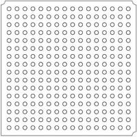
LFXP2-5E-5FTN256I Lattice, LFXP2-5E-5FTN256I Datasheet - Page 290

LFXP2-5E-5FTN256I
Manufacturer Part Number
LFXP2-5E-5FTN256I
Description
FPGA - Field Programmable Gate Array 5K LUTs 172 I/O Inst on DSP 1.2V -5 Spd
Manufacturer
Lattice
Datasheet
1.LFXP2-8E-5FTN256I.pdf
(341 pages)
Specifications of LFXP2-5E-5FTN256I
Number Of Macrocells
5000
Number Of Programmable I/os
172
Data Ram Size
169984
Supply Voltage (max)
1.26 V
Maximum Operating Temperature
+ 100 C
Minimum Operating Temperature
- 40 C
Mounting Style
SMD/SMT
Supply Voltage (min)
1.14 V
Package / Case
FTBGA-256
Number Of Logic Elements/cells
*
Number Of Labs/clbs
*
Total Ram Bits
169984
Number Of I /o
172
Number Of Gates
-
Voltage - Supply
1.14 V ~ 1.26 V
Mounting Type
*
Operating Temperature
-40°C ~ 100°C
Lead Free Status / RoHS Status
Lead free / RoHS Compliant
Available stocks
Company
Part Number
Manufacturer
Quantity
Price
Company:
Part Number:
LFXP2-5E-5FTN256I
Manufacturer:
Lattice
Quantity:
135
Company:
Part Number:
LFXP2-5E-5FTN256I
Manufacturer:
LATTICE
Quantity:
23
Company:
Part Number:
LFXP2-5E-5FTN256I
Manufacturer:
Lattice Semiconductor Corporation
Quantity:
10 000
Part Number:
LFXP2-5E-5FTN256I
Manufacturer:
LATTICE
Quantity:
20 000
- Current page: 290 of 341
- Download datasheet (10Mb)
Lattice Semiconductor
LatticeXP2 sysCONFIG Usage Guide
Flash Background programming may be used in both config mode and user mode (Done bit = 0 or 1). To support
Flash Background programming in user mode the SLAVE_SPI_PORT preference must be set to ENABLE.
When the CSSPISN pin goes low, the FPGA will wait for the preamble and then look for the proper commands. A
low on INITN indicates an error during a Flash erase or program. Data is written and read on the SISPI and SOSPI
pins.
After programming the Flash the user may toggle the PROGRAMN pin to transfer the Flash data to SRAM if the
SPI mode is being used. If the SDM mode is being used then the SRAM will be updated on the next power up
sequence of when a refresh instruction is issued.
If the CSSPISN pin is driven low, the CSSPIN should be driven high and CCLK maintained as an input to prevent
activating the Master SPI interface. This will avoid contention between the Master and Slave SPI interfaces.
ispJTAG Pins
The ispJTAG pins are standard IEEE 1149.1 TAP (Test Access Port) pins. The ispJTAG pins are dedicated pins and
are always accessible when the LatticeXP2 device is powered up. When programming the SRAM via ispJTAG the
dedicated programming pins, such as DONE, cannot be used to determine programming progress. This is because
the state of the boundary scan cell will drive the pin, per JTAG 1149.1, rather than normal internal logic.
TDO
The Test Data Output pin is used to shift out serial test instructions and data. When TDO is not being driven by the
internal circuitry, the pin will be in a high impedance state.
TDI
The Test Data Input pin is used to shift in serial test instructions and data. An internal pull-up resistor on the TDI pin
is provided. The internal resistor is pulled up to V
CCJ.
TMS
The Test Mode Select pin controls test operations on the TAP controller. On the falling edge of TCK, depending on
the state of TMS, a transition will be made in the TAP controller state machine. An internal pull-up resistor on the
TMS pin is provided. The internal resistor is pulled up to V
CCJ.
TCK
The test clock pin, TCK, provides the clock to run the TAP controller, which loads and unloads the data and instruc-
tion registers. TCK can be stopped in either the high or low state and can be clocked at frequencies up to the fre-
quency indicated in the device data sheet. The TCK pin supports the value is shown in the DC parameter table of
the data sheet. The TCK pin does not have a pull-up. A pull-down on the PCB of 4.7 K is recommended to avoid
inadvertent clocking of the TAP controller as V
ramps up.
CC
VCCJ
JTAG V
(V
) supplies independent power to the JTAG port to allow chaining with other JTAG devices at a com-
CC
CCJ
mon voltage. V
must be connected even if JTAG is not used. This voltage may also power the JTAG download
CCJ
cable. Valid voltage levels are 3.3V, 2.5V, 1.8V, 1.5V, and 1.2V.
Please see
In-System Programming Design Guidelines for ispJTAG Devices
for further information.
Configuration and JTAG Voltage Levels
All of the control pins and programming pins default to LVCMOS. The CFG0 pin is linked to V
(core); TCK, TDI,
CC
TDO, and TMS track V
; all other pins track the V
for that pin.
CCJ
CCIO
14-8
Related parts for LFXP2-5E-5FTN256I
Image
Part Number
Description
Manufacturer
Datasheet
Request
R

Part Number:
Description:
FPGA - Field Programmable Gate Array 5K LUTs 146I/O Inst- on DSP 1.2V -5 Spd
Manufacturer:
Lattice
Datasheet:

Part Number:
Description:
FPGA - Field Programmable Gate Array 5K LUTs 172I/O Inst- on DSP 1.2V -5 Spd
Manufacturer:
Lattice
Datasheet:

Part Number:
Description:
FPGA - Field Programmable Gate Array 5K LUTs 100 I/O Inst on DSP 1.2V -5 Spd
Manufacturer:
Lattice
Datasheet:

Part Number:
Description:
FPGA - Field Programmable Gate Array 5K LUTs 100I/O Inst- on DSP 1.2V -5 Spd
Manufacturer:
Lattice
Datasheet:
Part Number:
Description:
FPGA LatticeXP2 Family 5000 Cells Flash Technology 1.2V 256-Pin FTBGA
Manufacturer:
LATTICE SEMICONDUCTOR
Datasheet:
Part Number:
Description:
FPGA LatticeXP2 Family 5000 Cells Flash Technology 1.2V 256-Pin FTBGA
Manufacturer:
LATTICE SEMICONDUCTOR
Datasheet:

Part Number:
Description:
IC DSP 5KLUTS 100I/O 144TQFP
Manufacturer:
Lattice
Datasheet:

Part Number:
Description:
IC DSP 5KLUTS 86I/O 132CSBGA
Manufacturer:
Lattice
Datasheet:

Part Number:
Description:
IC DSP 5KLUTS 86I/O 132CSBGA
Manufacturer:
Lattice
Datasheet:

Part Number:
Description:
IC DSP 5KLUTS 146I/O 208PQFP
Manufacturer:
Lattice
Datasheet:

Part Number:
Description:
IC DSP 5KLUTS 146I/O 208PQFP
Manufacturer:
Lattice
Datasheet:

Part Number:
Description:
IC DSP 5KLUTS 172I/O 256FTBGA
Manufacturer:
Lattice
Datasheet:

Part Number:
Description:
IC FPGA 5KLUTS 86I/O 132-BGA
Manufacturer:
Lattice
Datasheet:

Part Number:
Description:
IC FPGA 5KLUTS 86I/O 132-BGA
Manufacturer:
Lattice
Datasheet:

Part Number:
Description:
IC FPGA 5KLUTS 86I/O 132-BGA
Manufacturer:
Lattice
Datasheet:


