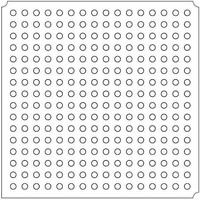
LFXP2-5E-5FTN256I Lattice, LFXP2-5E-5FTN256I Datasheet - Page 102

LFXP2-5E-5FTN256I
Manufacturer Part Number
LFXP2-5E-5FTN256I
Description
FPGA - Field Programmable Gate Array 5K LUTs 172 I/O Inst on DSP 1.2V -5 Spd
Manufacturer
Lattice
Datasheet
1.LFXP2-8E-5FTN256I.pdf
(341 pages)
Specifications of LFXP2-5E-5FTN256I
Number Of Macrocells
5000
Number Of Programmable I/os
172
Data Ram Size
169984
Supply Voltage (max)
1.26 V
Maximum Operating Temperature
+ 100 C
Minimum Operating Temperature
- 40 C
Mounting Style
SMD/SMT
Supply Voltage (min)
1.14 V
Package / Case
FTBGA-256
Number Of Logic Elements/cells
*
Number Of Labs/clbs
*
Total Ram Bits
169984
Number Of I /o
172
Number Of Gates
-
Voltage - Supply
1.14 V ~ 1.26 V
Mounting Type
*
Operating Temperature
-40°C ~ 100°C
Lead Free Status / RoHS Status
Lead free / RoHS Compliant
Available stocks
Company
Part Number
Manufacturer
Quantity
Price
Company:
Part Number:
LFXP2-5E-5FTN256I
Manufacturer:
Lattice
Quantity:
135
Company:
Part Number:
LFXP2-5E-5FTN256I
Manufacturer:
LATTICE
Quantity:
23
Company:
Part Number:
LFXP2-5E-5FTN256I
Manufacturer:
Lattice Semiconductor Corporation
Quantity:
10 000
Part Number:
LFXP2-5E-5FTN256I
Manufacturer:
LATTICE
Quantity:
20 000
- Current page: 102 of 341
- Download datasheet (10Mb)
www.latticesemi.com
© 2011 Lattice Semiconductor Corp. All Lattice trademarks, registered trademarks, patents, and disclaimers are as listed at www.latticesemi.com/legal. All other brand
or product names are trademarks or registered trademarks of their respective holders. The specifications and information herein are subject to change without notice.
April 2011
Revision History
September 2007
February 2008
April 2008
May 2007
Date
Version
01.1
01.2
01.3
01.4
Ordering Information
Pinout Information
Pinout Information
DC and Switching
DC and Switching
DC and Switching
Characteristics
Characteristics
Characteristics
Architecture
Section
—
Initial release.
Added JTAG Port Timing Waveforms diagram.
Updated sysCLOCK PLL Timing table.
Added Thermal Management text section.
Added LVCMOS33D to Supported Output Standards table.
Clarified: “This Flash can be programmed through either the JTAG or
Slave SPI ports of the device. The SRAM configuration space can also
be infinitely reconfigured through the JTAG and Master SPI ports.”
Added External Slave SPI Port to Serial TAG Memory section. Updated
Serial TAG Memory diagram.
Updated Flash Programming Specifications table.
Added “8W” specification to Hot Socketing Specifications table.
Updated Timing Tables
Clarifications for IIH in DC Electrical Characteristics table.
Added LVCMOS33D section
Updated DOA and DOA (Regs) to EBR Timing diagrams.
Removed Master Clock Frequency and Duty Cycle sections from the
LatticeXP2 sysCONFIG Port Timing Specifications table. These are
listed on the On-chip Oscillator and Configuration Master Clock Charac-
teristics table.
Changed CSSPIN to CSSPISN in description of t
parameters. Removed t
Clarified On-chip Oscillator documentation
Added Switching Test Conditions
Added “True LVDS Pairs Bonding Out per Bank,” “DDR Banks Bonding
Out per I/O Bank,” and “PCI capable I/Os Bonding Out per Bank” to Pin
Information Summary in place of previous blank table “PCI and DDR
Capabilities of the Device-Package Combinations”
Removed pinout listing. This information is available on the LatticeXP2
product web pages
Added XP2-17 “8W” and all other family OPNs.
Updated Absolute Maximum Ratings footnotes.
Updated Recommended Operating Conditions Table footnotes.
Updated Supply Current (Standby) Table
Updated Initialization Supply Current Table
Updated Programming and Erase Flash Supply Current Table
Updated Register to Register Performance Table
Updated LatticeXP2 External Switching Characteristics Table
Updated LatticeXP2 Internal Switching Characteristics Table
Updated sysCLOCK PLL Timing Table
LatticeXP2 Family Data Sheet
7-1
SOE
Change Summary
parameter.
Revision History
SCS
Data Sheet DS1009
, t
SCSS
, and t
SCSH
Related parts for LFXP2-5E-5FTN256I
Image
Part Number
Description
Manufacturer
Datasheet
Request
R

Part Number:
Description:
FPGA - Field Programmable Gate Array 5K LUTs 146I/O Inst- on DSP 1.2V -5 Spd
Manufacturer:
Lattice
Datasheet:

Part Number:
Description:
FPGA - Field Programmable Gate Array 5K LUTs 172I/O Inst- on DSP 1.2V -5 Spd
Manufacturer:
Lattice
Datasheet:

Part Number:
Description:
FPGA - Field Programmable Gate Array 5K LUTs 100 I/O Inst on DSP 1.2V -5 Spd
Manufacturer:
Lattice
Datasheet:

Part Number:
Description:
FPGA - Field Programmable Gate Array 5K LUTs 100I/O Inst- on DSP 1.2V -5 Spd
Manufacturer:
Lattice
Datasheet:
Part Number:
Description:
FPGA LatticeXP2 Family 5000 Cells Flash Technology 1.2V 256-Pin FTBGA
Manufacturer:
LATTICE SEMICONDUCTOR
Datasheet:
Part Number:
Description:
FPGA LatticeXP2 Family 5000 Cells Flash Technology 1.2V 256-Pin FTBGA
Manufacturer:
LATTICE SEMICONDUCTOR
Datasheet:

Part Number:
Description:
IC DSP 5KLUTS 100I/O 144TQFP
Manufacturer:
Lattice
Datasheet:

Part Number:
Description:
IC DSP 5KLUTS 86I/O 132CSBGA
Manufacturer:
Lattice
Datasheet:

Part Number:
Description:
IC DSP 5KLUTS 86I/O 132CSBGA
Manufacturer:
Lattice
Datasheet:

Part Number:
Description:
IC DSP 5KLUTS 146I/O 208PQFP
Manufacturer:
Lattice
Datasheet:

Part Number:
Description:
IC DSP 5KLUTS 146I/O 208PQFP
Manufacturer:
Lattice
Datasheet:

Part Number:
Description:
IC DSP 5KLUTS 172I/O 256FTBGA
Manufacturer:
Lattice
Datasheet:

Part Number:
Description:
IC FPGA 5KLUTS 86I/O 132-BGA
Manufacturer:
Lattice
Datasheet:

Part Number:
Description:
IC FPGA 5KLUTS 86I/O 132-BGA
Manufacturer:
Lattice
Datasheet:

Part Number:
Description:
IC FPGA 5KLUTS 86I/O 132-BGA
Manufacturer:
Lattice
Datasheet:


