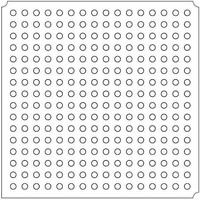
LFXP2-5E-5FTN256I Lattice, LFXP2-5E-5FTN256I Datasheet - Page 130

LFXP2-5E-5FTN256I
Manufacturer Part Number
LFXP2-5E-5FTN256I
Description
FPGA - Field Programmable Gate Array 5K LUTs 172 I/O Inst on DSP 1.2V -5 Spd
Manufacturer
Lattice
Datasheet
1.LFXP2-8E-5FTN256I.pdf
(341 pages)
Specifications of LFXP2-5E-5FTN256I
Number Of Macrocells
5000
Number Of Programmable I/os
172
Data Ram Size
169984
Supply Voltage (max)
1.26 V
Maximum Operating Temperature
+ 100 C
Minimum Operating Temperature
- 40 C
Mounting Style
SMD/SMT
Supply Voltage (min)
1.14 V
Package / Case
FTBGA-256
Number Of Logic Elements/cells
*
Number Of Labs/clbs
*
Total Ram Bits
169984
Number Of I /o
172
Number Of Gates
-
Voltage - Supply
1.14 V ~ 1.26 V
Mounting Type
*
Operating Temperature
-40°C ~ 100°C
Lead Free Status / RoHS Status
Lead free / RoHS Compliant
Available stocks
Company
Part Number
Manufacturer
Quantity
Price
Company:
Part Number:
LFXP2-5E-5FTN256I
Manufacturer:
Lattice
Quantity:
135
Company:
Part Number:
LFXP2-5E-5FTN256I
Manufacturer:
LATTICE
Quantity:
23
Company:
Part Number:
LFXP2-5E-5FTN256I
Manufacturer:
Lattice Semiconductor Corporation
Quantity:
10 000
Part Number:
LFXP2-5E-5FTN256I
Manufacturer:
LATTICE
Quantity:
20 000
- Current page: 130 of 341
- Download datasheet (10Mb)
Lattice Semiconductor
DUTY (Duty Cycle)
The DUTY attribute is used to select the Duty Cycle for CLKOS output. The Duty Cycle is programmable at 1/16th
of the period increment. Steps 2 to 14 are supported. 1/16th and 15/16th duty cycles are not supported to avoid the
minimum pulse width violation.
FB_MODE
There are three sources of feedback signals that can drive the CLKFB Divider: Internal, CLKOP (Clock Tree) and
user clock. CLKOP (Clock Tree) feedback is used by default. Internal feedback takes the CLKOP output at CLKOP
Divider output before the Clock Tree to minimize the feedback path delay. The user clock feedback is driven from
the dedicated pin, clock pin or user-specified internal logic.
DUTY_TRIM Adjustment (Dynamic mode only)
Users can fine tune the duty cycle of CLKOP and/or CLKOS with the DUTY_TRIM feature when Dynamic
PHASE/DUTY Adjustment is selected.
• TRIM Polarity Select: Users can select either rising edge or falling edge of clock to trim.
• TRIM Delay of CLKOP can be set to 0 to 7 steps of unit trim delay.
• TRIM Delay of CLKOS can be set to 0 to 3 steps of unit trim delay.
CLKOS/CLKOK/CLKOK2 Select
Users select these output clocks only when they are used in the design.
CLKOP/CLKOS/CLKOK BYPASS
These bypasses are enabled if set. CLKI is directly routed to its corresponding output clock.
RST/RSTK Select
Users may select these reset signals only when they are used in the design.
LatticeXP2 PLL Primitive Definition
One PLL primitive is used for LatticeXP2 PLL implementation. Figure 9-6 shows the LatticeXP2 PLL primitive
library symbols.
Figure 9-6. LatticeXP2 PLL Primitive Symbol
EPLLD Design Migration from LatticeECP2 to LatticeXP2
The EPLLD generated for LatticeECP2 can be used with minor changes. If the configuration does not include
Dynamic Phase and Duty Options, the migration is fully supported. If Dynamic Phase and Duty Options are
included, the user must tie the DPAMODE port to ground.
Dynamic Phase/Duty Mode
This mode sets both Dynamic Phase Adjustment and Dynamic Duty Select at the same time. There are two
modes, “Dynamic Phase and Dynamic Duty” and “Dynamic Phase and 50% Duty”.
Dynamic Phase and 50% Duty
This mode allows users to set up Dynamic Phase inputs only. The 50% Duty Cycle is handled internally by the isp-
LEVER
®
software. The DDUTY[3:0] ports are user-transparent in this mode.
RST
RSTK
CLKI
CLKFB
WRDEL
DPHASE[3:0]
DDUTY[3:]
EHXPLLE
9-8
CLKOK2
CLKOP
CLKOS
CLKOK
LOCK
LatticeXP2 sysCLOCK PLL
Design and Usage Guide
Related parts for LFXP2-5E-5FTN256I
Image
Part Number
Description
Manufacturer
Datasheet
Request
R

Part Number:
Description:
FPGA - Field Programmable Gate Array 5K LUTs 146I/O Inst- on DSP 1.2V -5 Spd
Manufacturer:
Lattice
Datasheet:

Part Number:
Description:
FPGA - Field Programmable Gate Array 5K LUTs 172I/O Inst- on DSP 1.2V -5 Spd
Manufacturer:
Lattice
Datasheet:

Part Number:
Description:
FPGA - Field Programmable Gate Array 5K LUTs 100 I/O Inst on DSP 1.2V -5 Spd
Manufacturer:
Lattice
Datasheet:

Part Number:
Description:
FPGA - Field Programmable Gate Array 5K LUTs 100I/O Inst- on DSP 1.2V -5 Spd
Manufacturer:
Lattice
Datasheet:
Part Number:
Description:
FPGA LatticeXP2 Family 5000 Cells Flash Technology 1.2V 256-Pin FTBGA
Manufacturer:
LATTICE SEMICONDUCTOR
Datasheet:
Part Number:
Description:
FPGA LatticeXP2 Family 5000 Cells Flash Technology 1.2V 256-Pin FTBGA
Manufacturer:
LATTICE SEMICONDUCTOR
Datasheet:

Part Number:
Description:
IC DSP 5KLUTS 100I/O 144TQFP
Manufacturer:
Lattice
Datasheet:

Part Number:
Description:
IC DSP 5KLUTS 86I/O 132CSBGA
Manufacturer:
Lattice
Datasheet:

Part Number:
Description:
IC DSP 5KLUTS 86I/O 132CSBGA
Manufacturer:
Lattice
Datasheet:

Part Number:
Description:
IC DSP 5KLUTS 146I/O 208PQFP
Manufacturer:
Lattice
Datasheet:

Part Number:
Description:
IC DSP 5KLUTS 146I/O 208PQFP
Manufacturer:
Lattice
Datasheet:

Part Number:
Description:
IC DSP 5KLUTS 172I/O 256FTBGA
Manufacturer:
Lattice
Datasheet:

Part Number:
Description:
IC FPGA 5KLUTS 86I/O 132-BGA
Manufacturer:
Lattice
Datasheet:

Part Number:
Description:
IC FPGA 5KLUTS 86I/O 132-BGA
Manufacturer:
Lattice
Datasheet:

Part Number:
Description:
IC FPGA 5KLUTS 86I/O 132-BGA
Manufacturer:
Lattice
Datasheet:


