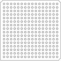
LFXP2-5E-5FTN256I Lattice, LFXP2-5E-5FTN256I Datasheet - Page 245

LFXP2-5E-5FTN256I
Manufacturer Part Number
LFXP2-5E-5FTN256I
Description
FPGA - Field Programmable Gate Array 5K LUTs 172 I/O Inst on DSP 1.2V -5 Spd
Manufacturer
Lattice
Datasheet
1.LFXP2-8E-5FTN256I.pdf
(341 pages)
Specifications of LFXP2-5E-5FTN256I
Number Of Macrocells
5000
Number Of Programmable I/os
172
Data Ram Size
169984
Supply Voltage (max)
1.26 V
Maximum Operating Temperature
+ 100 C
Minimum Operating Temperature
- 40 C
Mounting Style
SMD/SMT
Supply Voltage (min)
1.14 V
Package / Case
FTBGA-256
Number Of Logic Elements/cells
*
Number Of Labs/clbs
*
Total Ram Bits
169984
Number Of I /o
172
Number Of Gates
-
Voltage - Supply
1.14 V ~ 1.26 V
Mounting Type
*
Operating Temperature
-40°C ~ 100°C
Lead Free Status / RoHS Status
Lead free / RoHS Compliant
Available stocks
Company
Part Number
Manufacturer
Quantity
Price
Company:
Part Number:
LFXP2-5E-5FTN256I
Manufacturer:
Lattice
Quantity:
135
Company:
Part Number:
LFXP2-5E-5FTN256I
Manufacturer:
LATTICE
Quantity:
23
Company:
Part Number:
LFXP2-5E-5FTN256I
Manufacturer:
Lattice Semiconductor Corporation
Quantity:
10 000
Part Number:
LFXP2-5E-5FTN256I
Manufacturer:
LATTICE
Quantity:
20 000
- Current page: 245 of 341
- Download datasheet (10Mb)
February 2007
Introduction
One requirement for design engineers using programmable devices is the ability to calculate the power dissipation
for a particular device used on a board. Lattice’s ispLEVER
allows designers to calculate the power dissipation for a given device. This technical note describes how to use the
Power Calculator tool to calculate the power consumption of the LatticeXP2™ family of devices. General guidelines
to reduce power consumption are also included.
Power Supply Sequencing and Hot Socketing
LatticeXP2 devices have been designed to ensure predictable behavior during power-up and power-down. Power
supplies can be sequenced in any order. During power-up and power-down sequences, the I/Os remain in tri-state
until the power supply voltage is high enough to ensure reliable operation. In addition, leakage into I/O pins is con-
trolled to within the limits specified in the
of the system. These capabilities make the LatticeXP2 ideal for many multiple power supply and hot-swap applica-
tions.
Recommended Power-up Sequence
As described above, the supplies can be sequenced in any order. However, once internal power good is achieved
(determined by VCC, VCCAUX, VCCIO Bank x) the device releases the I/Os from tri-state and the management of
the I/Os becomes the designer's responsibility. To simplify a system design, it is recommended that supplies be
sequenced in the following order: VCCIO, VCC, VCCAUX. If VCCIO is tied to VCC or VCCAUX, then it is recom-
mended that VCCIO and the associated power supply are powered up before the remaining supply.
Please refer to the Hot Socketing section of the
Power Calculator Hardware Assumptions
Power consumption for a device can be coarsely broken down into the DC portion and the AC portion.
The Power Calculator reports the power dissipation in terms of:
The DC Power (or the Static power consumption) is the total power consumption of the used and the unused
resources. These power components are fixed for each resource used and depends upon the number of resource
units utilized. The DC component also includes the static power dissipation for the unused resources of the device.
The AC portion of power consumption is associated with the used resources. This is the dynamic part of the power
consumption. Its power dissipation is directly proportional to the frequency at which the resource is running and the
number of resource units used.
Power Calculation Equations
The following are the power equations used in the Power Calculator:
© 2007 Lattice Semiconductor Corp. All Lattice trademarks, registered trademarks, patents, and disclaimers are as listed at www.latticesemi.com/legal. All other brand
or product names are trademarks or registered trademarks of their respective holders. The specifications and information herein are subject to change without notice.
www.latticesemi.com
1. DC portion of the power consumption.
2. AC portion of the power consumption.
LatticeXP2 Family Data
Power Estimation and Management
LatticeXP2 Family Data Sheet
12-1
®
design tools include the Power Calculator tool, which
Sheet, allowing for easy integration with the rest
for LatticeXP2 Devices
for more information.
Technical Note TN1139
tn1139_01.0
Related parts for LFXP2-5E-5FTN256I
Image
Part Number
Description
Manufacturer
Datasheet
Request
R

Part Number:
Description:
FPGA - Field Programmable Gate Array 5K LUTs 146I/O Inst- on DSP 1.2V -5 Spd
Manufacturer:
Lattice
Datasheet:

Part Number:
Description:
FPGA - Field Programmable Gate Array 5K LUTs 172I/O Inst- on DSP 1.2V -5 Spd
Manufacturer:
Lattice
Datasheet:

Part Number:
Description:
FPGA - Field Programmable Gate Array 5K LUTs 100 I/O Inst on DSP 1.2V -5 Spd
Manufacturer:
Lattice
Datasheet:

Part Number:
Description:
FPGA - Field Programmable Gate Array 5K LUTs 100I/O Inst- on DSP 1.2V -5 Spd
Manufacturer:
Lattice
Datasheet:
Part Number:
Description:
FPGA LatticeXP2 Family 5000 Cells Flash Technology 1.2V 256-Pin FTBGA
Manufacturer:
LATTICE SEMICONDUCTOR
Datasheet:
Part Number:
Description:
FPGA LatticeXP2 Family 5000 Cells Flash Technology 1.2V 256-Pin FTBGA
Manufacturer:
LATTICE SEMICONDUCTOR
Datasheet:

Part Number:
Description:
IC DSP 5KLUTS 100I/O 144TQFP
Manufacturer:
Lattice
Datasheet:

Part Number:
Description:
IC DSP 5KLUTS 86I/O 132CSBGA
Manufacturer:
Lattice
Datasheet:

Part Number:
Description:
IC DSP 5KLUTS 86I/O 132CSBGA
Manufacturer:
Lattice
Datasheet:

Part Number:
Description:
IC DSP 5KLUTS 146I/O 208PQFP
Manufacturer:
Lattice
Datasheet:

Part Number:
Description:
IC DSP 5KLUTS 146I/O 208PQFP
Manufacturer:
Lattice
Datasheet:

Part Number:
Description:
IC DSP 5KLUTS 172I/O 256FTBGA
Manufacturer:
Lattice
Datasheet:

Part Number:
Description:
IC FPGA 5KLUTS 86I/O 132-BGA
Manufacturer:
Lattice
Datasheet:

Part Number:
Description:
IC FPGA 5KLUTS 86I/O 132-BGA
Manufacturer:
Lattice
Datasheet:

Part Number:
Description:
IC FPGA 5KLUTS 86I/O 132-BGA
Manufacturer:
Lattice
Datasheet:


