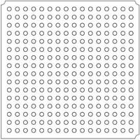
LFXP2-5E-5FTN256I Lattice, LFXP2-5E-5FTN256I Datasheet - Page 309

LFXP2-5E-5FTN256I
Manufacturer Part Number
LFXP2-5E-5FTN256I
Description
FPGA - Field Programmable Gate Array 5K LUTs 172 I/O Inst on DSP 1.2V -5 Spd
Manufacturer
Lattice
Datasheet
1.LFXP2-8E-5FTN256I.pdf
(341 pages)
Specifications of LFXP2-5E-5FTN256I
Number Of Macrocells
5000
Number Of Programmable I/os
172
Data Ram Size
169984
Supply Voltage (max)
1.26 V
Maximum Operating Temperature
+ 100 C
Minimum Operating Temperature
- 40 C
Mounting Style
SMD/SMT
Supply Voltage (min)
1.14 V
Package / Case
FTBGA-256
Number Of Logic Elements/cells
*
Number Of Labs/clbs
*
Total Ram Bits
169984
Number Of I /o
172
Number Of Gates
-
Voltage - Supply
1.14 V ~ 1.26 V
Mounting Type
*
Operating Temperature
-40°C ~ 100°C
Lead Free Status / RoHS Status
Lead free / RoHS Compliant
Available stocks
Company
Part Number
Manufacturer
Quantity
Price
Company:
Part Number:
LFXP2-5E-5FTN256I
Manufacturer:
Lattice
Quantity:
135
Company:
Part Number:
LFXP2-5E-5FTN256I
Manufacturer:
LATTICE
Quantity:
23
Company:
Part Number:
LFXP2-5E-5FTN256I
Manufacturer:
Lattice Semiconductor Corporation
Quantity:
10 000
Part Number:
LFXP2-5E-5FTN256I
Manufacturer:
LATTICE
Quantity:
20 000
- Current page: 309 of 341
- Download datasheet (10Mb)
September 2009
Introduction
Soft errors occur when high-energy charged particles alter the stored charge in a memory cell in an electronic cir-
cuit. The phenomenon first became an issue in DRAM, requiring error detection and correction for large memory
systems in high-reliability applications. As device geometries have continued to shrink, the probability of soft errors
in SRAM has become significant for some systems. Designers are using a variety of approaches to minimize the
effects of soft errors on system behavior.
SRAM-based FPGAs store logic configuration data in SRAM cells. As the number and density of SRAM cells in an
FPGA increase, the probability that a soft error will alter the programmed logical behavior of the system increases.
A number of approaches have been taken to address this issue, but most involve Intellectual Property (IP) cores
that the user instantiates into the logic of their design, using valuable resources and possibly affecting design per-
formance. The LatticeXP2 devices have a hardware implemented soft error detector which does not affect perfor-
mance or heat dissipation of the devices.
This document describes the hardware based soft error detect (SED) approach taken by Lattice Semiconductor for
LatticeXP2™ FPGAs.
SED Overview
The SED hardware in the LatticeXP2 devices consists of an access point to FPGA configuration memory, a control-
ler circuit, and a 32-bit register to store the CRC for a given bitstream (see Figure 16-1). The SED hardware reads
serial data from the FPGA’s configuration memory and calculates a CRC. The data that is read, and the CRC that
is calculated, does not include EBR memory or PFUs used as RAM. The calculated CRC is then compared with
the expected CRC that was stored in the 32-bit register. If the CRC values match it indicates that there has been no
configuration memory corruption, but if the values differ an error signal is generated. SED checking does not
impact the performance or operation of the user logic.
Figure 16-1. System Block Diagram
© 2009 Lattice Semiconductor Corp. All Lattice trademarks, registered trademarks, patents, and disclaimers are as listed at www.latticesemi.com/legal. All other brand
or product names are trademarks or registered trademarks of their respective holders. The specifications and information herein are subject to change without notice.
www.latticesemi.com
Logic
User
LatticeXP2
16-1
Detection (SED) Usage Guide
CRC Register
Internal Flash
Logic Access
SED Control
Config Logic
Circuit
32-Bit
OSC
LatticeXP2 Soft Error
Technical Note TN1130
tn1130_02.0
Related parts for LFXP2-5E-5FTN256I
Image
Part Number
Description
Manufacturer
Datasheet
Request
R

Part Number:
Description:
FPGA - Field Programmable Gate Array 5K LUTs 146I/O Inst- on DSP 1.2V -5 Spd
Manufacturer:
Lattice
Datasheet:

Part Number:
Description:
FPGA - Field Programmable Gate Array 5K LUTs 172I/O Inst- on DSP 1.2V -5 Spd
Manufacturer:
Lattice
Datasheet:

Part Number:
Description:
FPGA - Field Programmable Gate Array 5K LUTs 100 I/O Inst on DSP 1.2V -5 Spd
Manufacturer:
Lattice
Datasheet:

Part Number:
Description:
FPGA - Field Programmable Gate Array 5K LUTs 100I/O Inst- on DSP 1.2V -5 Spd
Manufacturer:
Lattice
Datasheet:
Part Number:
Description:
FPGA LatticeXP2 Family 5000 Cells Flash Technology 1.2V 256-Pin FTBGA
Manufacturer:
LATTICE SEMICONDUCTOR
Datasheet:
Part Number:
Description:
FPGA LatticeXP2 Family 5000 Cells Flash Technology 1.2V 256-Pin FTBGA
Manufacturer:
LATTICE SEMICONDUCTOR
Datasheet:

Part Number:
Description:
IC DSP 5KLUTS 100I/O 144TQFP
Manufacturer:
Lattice
Datasheet:

Part Number:
Description:
IC DSP 5KLUTS 86I/O 132CSBGA
Manufacturer:
Lattice
Datasheet:

Part Number:
Description:
IC DSP 5KLUTS 86I/O 132CSBGA
Manufacturer:
Lattice
Datasheet:

Part Number:
Description:
IC DSP 5KLUTS 146I/O 208PQFP
Manufacturer:
Lattice
Datasheet:

Part Number:
Description:
IC DSP 5KLUTS 146I/O 208PQFP
Manufacturer:
Lattice
Datasheet:

Part Number:
Description:
IC DSP 5KLUTS 172I/O 256FTBGA
Manufacturer:
Lattice
Datasheet:

Part Number:
Description:
IC FPGA 5KLUTS 86I/O 132-BGA
Manufacturer:
Lattice
Datasheet:

Part Number:
Description:
IC FPGA 5KLUTS 86I/O 132-BGA
Manufacturer:
Lattice
Datasheet:

Part Number:
Description:
IC FPGA 5KLUTS 86I/O 132-BGA
Manufacturer:
Lattice
Datasheet:


