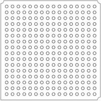
LFXP2-5E-5FTN256I Lattice, LFXP2-5E-5FTN256I Datasheet - Page 205

LFXP2-5E-5FTN256I
Manufacturer Part Number
LFXP2-5E-5FTN256I
Description
FPGA - Field Programmable Gate Array 5K LUTs 172 I/O Inst on DSP 1.2V -5 Spd
Manufacturer
Lattice
Datasheet
1.LFXP2-8E-5FTN256I.pdf
(341 pages)
Specifications of LFXP2-5E-5FTN256I
Number Of Macrocells
5000
Number Of Programmable I/os
172
Data Ram Size
169984
Supply Voltage (max)
1.26 V
Maximum Operating Temperature
+ 100 C
Minimum Operating Temperature
- 40 C
Mounting Style
SMD/SMT
Supply Voltage (min)
1.14 V
Package / Case
FTBGA-256
Number Of Logic Elements/cells
*
Number Of Labs/clbs
*
Total Ram Bits
169984
Number Of I /o
172
Number Of Gates
-
Voltage - Supply
1.14 V ~ 1.26 V
Mounting Type
*
Operating Temperature
-40°C ~ 100°C
Lead Free Status / RoHS Status
Lead free / RoHS Compliant
Available stocks
Company
Part Number
Manufacturer
Quantity
Price
Company:
Part Number:
LFXP2-5E-5FTN256I
Manufacturer:
Lattice
Quantity:
135
Company:
Part Number:
LFXP2-5E-5FTN256I
Manufacturer:
LATTICE
Quantity:
23
Company:
Part Number:
LFXP2-5E-5FTN256I
Manufacturer:
Lattice Semiconductor Corporation
Quantity:
10 000
Part Number:
LFXP2-5E-5FTN256I
Manufacturer:
LATTICE
Quantity:
20 000
- Current page: 205 of 341
- Download datasheet (10Mb)
LatticeXP2 High-Speed I/O Interface
June 2009
Technical Note TN1138
Introduction
LatticeXP2™ devices support Double Data Rate (DDR) and Single Data Rate (SDR) interfaces using the logic built
into the Programmable I/O (PIO). SDR applications capture data on one edge of a clock while the DDR interfaces
capture data on both the rising and falling edges of the clock, thus doubling performance. The LatticeXP2 I/Os also
have dedicated circuitry to support DDR and DDR2 SDRAM memory interfaces. This technical note details the use
of LatticeXP2 devices to implement both a high-speed generic DDR interface and DDR and DDR2 memory inter-
faces.
DDR and DDR2 SDRAM Interfaces Overview
A DDR SDRAM interface will transfer data at both the rising and falling edges of the clock. The DDR2 is the second
generation of the DDR SRDRAM memory.
The DDR and DDR2 SDRAM interfaces rely on the use of a data strobe signal, called DQS, for high-speed opera-
tion. The DDR SDRAM interface uses a single-ended DQS strobe signal, whereas the DDR2 interface uses a dif-
ferential DQS strobe. Figures 11-1 and 11-2 show typical DDR and DDR2 SDRAM interface signals. SDRAM
interfaces are typically implemented with eight DQ data bits per DQS. An x16 interface will use two DQS signals
and each DQS is associated with eight DQ bits. Both the DQ and DQS are bi-directional ports used to both read
and write to the memory.
When reading data from the external memory device, data coming into the device is edge-aligned with respect to
the DQS signal. This DQS strobe signal needs to be phase-shifted 90 degrees before FPGA logic can sample the
read data. When writing to a DDR/DDR2 SDRAM, the memory controller (FPGA) must shift the DQS by 90
degrees to center-align with the data signals (DQ). A clock signal is also provided to the memory. This clock is pro-
vided as a differential clock (CLKP and CLKN) to minimize duty cycle variations. The memory also uses these
clock signals to generate the DQS signal during a read via a DLL inside the memory. Figures 11-3 and 11-4 show
DQ and DQS timing relationships for read and write cycles. For other detailed timing requirements, please refer to
the DDR SDRAM JEDEC specification (JESD79C).
During read, the DQS signal is LOW for some duration after it comes out of tristate. This state is called Preamble.
The state when the DQS is LOW before it goes into Tristate is the Postamble state. This is the state after the last
valid data transition.
DDR SDRAM also requires a Data Mask (DM) signal to mask data bits during write cycles. Note that the ratio of
DQS to data bits is independent of the overall width of the memory. An 8-bit interface will have one strobe signal.
DDR SDRAM interfaces use the SSTL25 Class I/II I/O standards whereas the DDR2 SDRAM interface uses the
SSTL18 Class I/II I/O standards. The DDR2 SDRAM interface also supports differential DQS (DQS and DQS#).
© 2009 Lattice Semiconductor Corp. All Lattice trademarks, registered trademarks, patents, and disclaimers are as listed at www.latticesemi.com/legal. All other brand
or product names are trademarks or registered trademarks of their respective holders. The specifications and information herein are subject to change without notice.
www.latticesemi.com
11-1
tn1138_01.3
Related parts for LFXP2-5E-5FTN256I
Image
Part Number
Description
Manufacturer
Datasheet
Request
R

Part Number:
Description:
FPGA - Field Programmable Gate Array 5K LUTs 146I/O Inst- on DSP 1.2V -5 Spd
Manufacturer:
Lattice
Datasheet:

Part Number:
Description:
FPGA - Field Programmable Gate Array 5K LUTs 172I/O Inst- on DSP 1.2V -5 Spd
Manufacturer:
Lattice
Datasheet:

Part Number:
Description:
FPGA - Field Programmable Gate Array 5K LUTs 100 I/O Inst on DSP 1.2V -5 Spd
Manufacturer:
Lattice
Datasheet:

Part Number:
Description:
FPGA - Field Programmable Gate Array 5K LUTs 100I/O Inst- on DSP 1.2V -5 Spd
Manufacturer:
Lattice
Datasheet:
Part Number:
Description:
FPGA LatticeXP2 Family 5000 Cells Flash Technology 1.2V 256-Pin FTBGA
Manufacturer:
LATTICE SEMICONDUCTOR
Datasheet:
Part Number:
Description:
FPGA LatticeXP2 Family 5000 Cells Flash Technology 1.2V 256-Pin FTBGA
Manufacturer:
LATTICE SEMICONDUCTOR
Datasheet:

Part Number:
Description:
IC DSP 5KLUTS 100I/O 144TQFP
Manufacturer:
Lattice
Datasheet:

Part Number:
Description:
IC DSP 5KLUTS 86I/O 132CSBGA
Manufacturer:
Lattice
Datasheet:

Part Number:
Description:
IC DSP 5KLUTS 86I/O 132CSBGA
Manufacturer:
Lattice
Datasheet:

Part Number:
Description:
IC DSP 5KLUTS 146I/O 208PQFP
Manufacturer:
Lattice
Datasheet:

Part Number:
Description:
IC DSP 5KLUTS 146I/O 208PQFP
Manufacturer:
Lattice
Datasheet:

Part Number:
Description:
IC DSP 5KLUTS 172I/O 256FTBGA
Manufacturer:
Lattice
Datasheet:

Part Number:
Description:
IC FPGA 5KLUTS 86I/O 132-BGA
Manufacturer:
Lattice
Datasheet:

Part Number:
Description:
IC FPGA 5KLUTS 86I/O 132-BGA
Manufacturer:
Lattice
Datasheet:

Part Number:
Description:
IC FPGA 5KLUTS 86I/O 132-BGA
Manufacturer:
Lattice
Datasheet:


