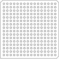
LFXP2-5E-5FTN256I Lattice, LFXP2-5E-5FTN256I Datasheet - Page 313

LFXP2-5E-5FTN256I
Manufacturer Part Number
LFXP2-5E-5FTN256I
Description
FPGA - Field Programmable Gate Array 5K LUTs 172 I/O Inst on DSP 1.2V -5 Spd
Manufacturer
Lattice
Datasheet
1.LFXP2-8E-5FTN256I.pdf
(341 pages)
Specifications of LFXP2-5E-5FTN256I
Number Of Macrocells
5000
Number Of Programmable I/os
172
Data Ram Size
169984
Supply Voltage (max)
1.26 V
Maximum Operating Temperature
+ 100 C
Minimum Operating Temperature
- 40 C
Mounting Style
SMD/SMT
Supply Voltage (min)
1.14 V
Package / Case
FTBGA-256
Number Of Logic Elements/cells
*
Number Of Labs/clbs
*
Total Ram Bits
169984
Number Of I /o
172
Number Of Gates
-
Voltage - Supply
1.14 V ~ 1.26 V
Mounting Type
*
Operating Temperature
-40°C ~ 100°C
Lead Free Status / RoHS Status
Lead free / RoHS Compliant
Available stocks
Company
Part Number
Manufacturer
Quantity
Price
Company:
Part Number:
LFXP2-5E-5FTN256I
Manufacturer:
Lattice
Quantity:
135
Company:
Part Number:
LFXP2-5E-5FTN256I
Manufacturer:
LATTICE
Quantity:
23
Company:
Part Number:
LFXP2-5E-5FTN256I
Manufacturer:
Lattice Semiconductor Corporation
Quantity:
10 000
Part Number:
LFXP2-5E-5FTN256I
Manufacturer:
LATTICE
Quantity:
20 000
- Current page: 313 of 341
- Download datasheet (10Mb)
Lattice Semiconductor
The general SED flow is as follows.
The user has two choices when an error is detected, ignore the error, and possibly log it, or reconfigure the FPGA.
Reconfiguration can be accomplished by driving the PROGRAMN pin low. This can be done by externally connect-
ing a GPIO pin to PROGRAMN.
Figure 16-4. Example Schematic
SED Run Time
The amount of time needed to perform an SED check depends on the density of the device and the frequency of
SEDCLKIN. There will also be some overhead time for calculation, but it is fairly short in comparison. An approxi-
mation of the time required can be found by using the following formula:
Maxbits is in mega-bits and depends on the density of the FPGA (see Table 16-8). SEDCLKIN is frequency in MHz.
Time is in seconds
For example, for a design using a LatticeXP2 with 5K look-up tables and the SEDCLKIN is the software default of
3.1 MHz:
In this example, SED checking will take approximately 398.71 ms. Remember that this happens in the background
and does not affect user logic performance.
Note that the internal oscillator used to generate SEDCLKIN can vary by ±30%.
1. User logic sets SEDENABLE high. This signal may be tied high if desired.
2. User logic sets SEDSTART high. SEDINPROG goes high. If SEDDONE is already high it is driven low.
3. SED starts reading back data from the configuration SRAM.
4. SED finishes checking. SEDERR is updated, SEDINPROG goes low, and SEDDONE goes high.
5. If SEDERR is driven high there are only two ways to reset it, drive SEDENABLE low or reconfigure the
6. SEDENABLE goes low when/if the user specifies, and SED is no longer in use.
SEDSTART may be tied high to enable continuous SED checking.
FPGA.
Maxbits / SEDCLKIN = Time
1.236 Mbits / 3.1 MHz = 398.71 ms
LatticeXP2
PROGRAMN
GPIO
16-5
VCC
Open Drain
Output
10K
Detection Usage Guide
LatticeXP2 Soft Error
Related parts for LFXP2-5E-5FTN256I
Image
Part Number
Description
Manufacturer
Datasheet
Request
R

Part Number:
Description:
FPGA - Field Programmable Gate Array 5K LUTs 146I/O Inst- on DSP 1.2V -5 Spd
Manufacturer:
Lattice
Datasheet:

Part Number:
Description:
FPGA - Field Programmable Gate Array 5K LUTs 172I/O Inst- on DSP 1.2V -5 Spd
Manufacturer:
Lattice
Datasheet:

Part Number:
Description:
FPGA - Field Programmable Gate Array 5K LUTs 100 I/O Inst on DSP 1.2V -5 Spd
Manufacturer:
Lattice
Datasheet:

Part Number:
Description:
FPGA - Field Programmable Gate Array 5K LUTs 100I/O Inst- on DSP 1.2V -5 Spd
Manufacturer:
Lattice
Datasheet:
Part Number:
Description:
FPGA LatticeXP2 Family 5000 Cells Flash Technology 1.2V 256-Pin FTBGA
Manufacturer:
LATTICE SEMICONDUCTOR
Datasheet:
Part Number:
Description:
FPGA LatticeXP2 Family 5000 Cells Flash Technology 1.2V 256-Pin FTBGA
Manufacturer:
LATTICE SEMICONDUCTOR
Datasheet:

Part Number:
Description:
IC DSP 5KLUTS 100I/O 144TQFP
Manufacturer:
Lattice
Datasheet:

Part Number:
Description:
IC DSP 5KLUTS 86I/O 132CSBGA
Manufacturer:
Lattice
Datasheet:

Part Number:
Description:
IC DSP 5KLUTS 86I/O 132CSBGA
Manufacturer:
Lattice
Datasheet:

Part Number:
Description:
IC DSP 5KLUTS 146I/O 208PQFP
Manufacturer:
Lattice
Datasheet:

Part Number:
Description:
IC DSP 5KLUTS 146I/O 208PQFP
Manufacturer:
Lattice
Datasheet:

Part Number:
Description:
IC DSP 5KLUTS 172I/O 256FTBGA
Manufacturer:
Lattice
Datasheet:

Part Number:
Description:
IC FPGA 5KLUTS 86I/O 132-BGA
Manufacturer:
Lattice
Datasheet:

Part Number:
Description:
IC FPGA 5KLUTS 86I/O 132-BGA
Manufacturer:
Lattice
Datasheet:

Part Number:
Description:
IC FPGA 5KLUTS 86I/O 132-BGA
Manufacturer:
Lattice
Datasheet:


