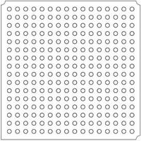
LFXP2-5E-5FTN256I Lattice, LFXP2-5E-5FTN256I Datasheet - Page 226

LFXP2-5E-5FTN256I
Manufacturer Part Number
LFXP2-5E-5FTN256I
Description
FPGA - Field Programmable Gate Array 5K LUTs 172 I/O Inst on DSP 1.2V -5 Spd
Manufacturer
Lattice
Datasheet
1.LFXP2-8E-5FTN256I.pdf
(341 pages)
Specifications of LFXP2-5E-5FTN256I
Number Of Macrocells
5000
Number Of Programmable I/os
172
Data Ram Size
169984
Supply Voltage (max)
1.26 V
Maximum Operating Temperature
+ 100 C
Minimum Operating Temperature
- 40 C
Mounting Style
SMD/SMT
Supply Voltage (min)
1.14 V
Package / Case
FTBGA-256
Number Of Logic Elements/cells
*
Number Of Labs/clbs
*
Total Ram Bits
169984
Number Of I /o
172
Number Of Gates
-
Voltage - Supply
1.14 V ~ 1.26 V
Mounting Type
*
Operating Temperature
-40°C ~ 100°C
Lead Free Status / RoHS Status
Lead free / RoHS Compliant
Available stocks
Company
Part Number
Manufacturer
Quantity
Price
Company:
Part Number:
LFXP2-5E-5FTN256I
Manufacturer:
Lattice
Quantity:
135
Company:
Part Number:
LFXP2-5E-5FTN256I
Manufacturer:
LATTICE
Quantity:
23
Company:
Part Number:
LFXP2-5E-5FTN256I
Manufacturer:
Lattice Semiconductor Corporation
Quantity:
10 000
Part Number:
LFXP2-5E-5FTN256I
Manufacturer:
LATTICE
Quantity:
20 000
- Current page: 226 of 341
- Download datasheet (10Mb)
Lattice Semiconductor
Write Timing Waveforms
Figure 11-25 shows the DDR write side data transfer timing for the DQ Data pad and the DQS Strobe Pad. When
writing to the DDR memory device, the DM (Data Mask) and the ADDR/ CMD (Address and Command) signals are
also sent to the memory device along with the data and strobe signals.
Figure 11-25. DDR Write Data Transfer for DQ Data
Design Rules/Guidelines
Listed below are some rules and guidelines to keep in mind when implementing DDR memory interfaces in the
LatticeXP2 devices.
• The LatticeXP2 devices have dedicated DQ-DQS banks. Please refer to the logical signal connections of the
• There are two DQSDLL on the device, one for the left half and one for the right half of the device. Therefore, only
• When implementing a DDR SDRAM interface, all interface signals should be connected to the SSTL25 I/O stan-
• For DDR2, the differential DQS signals need to be connected to SSTL18 the Differential I/O standard.
• When implementing the DDR interface, the VREF1 of the bank is used to provide the reference voltage for the
Generic High Speed DDR Implementation
In addition to the DDR memory interface, the I/O logic DDR registers can be used to implement high speed DDR
interfaces. The Input DDR registers can operate in full clock transfer and half clock transfer modes. The DDR input
and output register also support x1 and x2 gearing ratios. A gearing capability is provided to Mux/DeMux the I/O
data rate (ECLK) to the FPGA clock rate (SCLK). For DDR interfaces, this ratio is slightly different than the SDR
ratio. A basic 2x DDR element provides four FPGA side bits for two I/O side bits at half the clock rate on the FPGA
side.
groups in the
one DQSDLL primitive should be instantiated for each half of the device. Since there is only one DQSDLL on
each half of the device, all the DDR memory interfaces on that half of the device should run at the same fre-
quency. Each of the DQSDLL will generate 90-degree digital delay bits for all the DQS delay blocks on that half of
the device based on the reference clock input to the DLL.
dard. In the case of the DDR2 SDRAM interface, the interface signal should be connected to SSTL18 I/O stan-
dard.
interface pins.
DQSXFER
ECLK
CLKN
CLKP
DQS
DQ
DA
DB
LatticeXP2 Family Data Sheet
XX
P0
N0
P0
N0
P1
N1
before locking these pins.
P1
11-22
N1
N2
P2
P2
LatticeXP2 High-Speed I/O Interface
N2
N3
P3
P3
N3
N4
P4
P4
..
..
..
Related parts for LFXP2-5E-5FTN256I
Image
Part Number
Description
Manufacturer
Datasheet
Request
R

Part Number:
Description:
FPGA - Field Programmable Gate Array 5K LUTs 146I/O Inst- on DSP 1.2V -5 Spd
Manufacturer:
Lattice
Datasheet:

Part Number:
Description:
FPGA - Field Programmable Gate Array 5K LUTs 172I/O Inst- on DSP 1.2V -5 Spd
Manufacturer:
Lattice
Datasheet:

Part Number:
Description:
FPGA - Field Programmable Gate Array 5K LUTs 100 I/O Inst on DSP 1.2V -5 Spd
Manufacturer:
Lattice
Datasheet:

Part Number:
Description:
FPGA - Field Programmable Gate Array 5K LUTs 100I/O Inst- on DSP 1.2V -5 Spd
Manufacturer:
Lattice
Datasheet:
Part Number:
Description:
FPGA LatticeXP2 Family 5000 Cells Flash Technology 1.2V 256-Pin FTBGA
Manufacturer:
LATTICE SEMICONDUCTOR
Datasheet:
Part Number:
Description:
FPGA LatticeXP2 Family 5000 Cells Flash Technology 1.2V 256-Pin FTBGA
Manufacturer:
LATTICE SEMICONDUCTOR
Datasheet:

Part Number:
Description:
IC DSP 5KLUTS 100I/O 144TQFP
Manufacturer:
Lattice
Datasheet:

Part Number:
Description:
IC DSP 5KLUTS 86I/O 132CSBGA
Manufacturer:
Lattice
Datasheet:

Part Number:
Description:
IC DSP 5KLUTS 86I/O 132CSBGA
Manufacturer:
Lattice
Datasheet:

Part Number:
Description:
IC DSP 5KLUTS 146I/O 208PQFP
Manufacturer:
Lattice
Datasheet:

Part Number:
Description:
IC DSP 5KLUTS 146I/O 208PQFP
Manufacturer:
Lattice
Datasheet:

Part Number:
Description:
IC DSP 5KLUTS 172I/O 256FTBGA
Manufacturer:
Lattice
Datasheet:

Part Number:
Description:
IC FPGA 5KLUTS 86I/O 132-BGA
Manufacturer:
Lattice
Datasheet:

Part Number:
Description:
IC FPGA 5KLUTS 86I/O 132-BGA
Manufacturer:
Lattice
Datasheet:

Part Number:
Description:
IC FPGA 5KLUTS 86I/O 132-BGA
Manufacturer:
Lattice
Datasheet:


