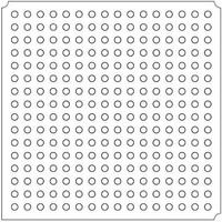
LFXP2-5E-5FTN256I Lattice, LFXP2-5E-5FTN256I Datasheet - Page 211

LFXP2-5E-5FTN256I
Manufacturer Part Number
LFXP2-5E-5FTN256I
Description
FPGA - Field Programmable Gate Array 5K LUTs 172 I/O Inst on DSP 1.2V -5 Spd
Manufacturer
Lattice
Datasheet
1.LFXP2-8E-5FTN256I.pdf
(341 pages)
Specifications of LFXP2-5E-5FTN256I
Number Of Macrocells
5000
Number Of Programmable I/os
172
Data Ram Size
169984
Supply Voltage (max)
1.26 V
Maximum Operating Temperature
+ 100 C
Minimum Operating Temperature
- 40 C
Mounting Style
SMD/SMT
Supply Voltage (min)
1.14 V
Package / Case
FTBGA-256
Number Of Logic Elements/cells
*
Number Of Labs/clbs
*
Total Ram Bits
169984
Number Of I /o
172
Number Of Gates
-
Voltage - Supply
1.14 V ~ 1.26 V
Mounting Type
*
Operating Temperature
-40°C ~ 100°C
Lead Free Status / RoHS Status
Lead free / RoHS Compliant
Available stocks
Company
Part Number
Manufacturer
Quantity
Price
Company:
Part Number:
LFXP2-5E-5FTN256I
Manufacturer:
Lattice
Quantity:
135
Company:
Part Number:
LFXP2-5E-5FTN256I
Manufacturer:
LATTICE
Quantity:
23
Company:
Part Number:
LFXP2-5E-5FTN256I
Manufacturer:
Lattice Semiconductor Corporation
Quantity:
10 000
Part Number:
LFXP2-5E-5FTN256I
Manufacturer:
LATTICE
Quantity:
20 000
- Current page: 211 of 341
- Download datasheet (10Mb)
Lattice Semiconductor
Table 11-2. DQSBUFC Ports
READ Pulse Generation
The READ signal to the DQSBUFC block is internally generated in the FPGA core. The READ signal goes high
when the READ command to control the DDR-SDRAM is initially asserted. This precedes the DQS preamble by
one cycle, yet may overlap the trailing bits of a prior read cycle. The DQS Detect circuitry of the LatticeXP2 device
requires the falling edge of the READ signal to be placed within the preamble stage.
The preamble state of the DQS can be detected using the CAS latency and the round trip delay for the signals
between the FPGA and the memory device. Note that the internal FPGA core generates the READ pulse. The rise
of the READ pulse should coincide with the initial READ command of the Read Burst and need to go low before the
Preamble goes high.
Figure 11-9 shows a READ Pulse timing example with respect to the PRMBDET signal.
Figure 11-9. READ Pulse Generation
OK
FAIL
FAIL
OK
PRMBDET
DQSI
CLK
READ
DQSDEL
XCLK
DQSO
DQSC
DDRCLKPOL
PRMBDET
DQSXFER
DATAVALID
READ
READ
READ
READ
Port Name
DQS
PRIOR READ CYCLE
I/O
O
O
O
O
O
O
I
I
I
I
I
POSTAMBLE
DQS Strobe signal from memory
System CLK
Read generated from the FPGA core
DQS Delay from the DQSDLL primitive
Edge Clock or System CLK
Delayed DQS Strobe signal, to the input capture register block
DQS Strobe signal before delay, going to the FPGA core logic
DDR Clock Polarity signal
Preamble detect signal, going to the FPGA core logic
90 degree shifted clock going to the Output DDR register Block
Signal indicating transmission of Valid data to the FPGA core
PREAMBLE
VTH
11-7
TRANSITION
FIRST DQS
Description
LatticeXP2 High-Speed I/O Interface
POSTAMBLE
Related parts for LFXP2-5E-5FTN256I
Image
Part Number
Description
Manufacturer
Datasheet
Request
R

Part Number:
Description:
FPGA - Field Programmable Gate Array 5K LUTs 146I/O Inst- on DSP 1.2V -5 Spd
Manufacturer:
Lattice
Datasheet:

Part Number:
Description:
FPGA - Field Programmable Gate Array 5K LUTs 172I/O Inst- on DSP 1.2V -5 Spd
Manufacturer:
Lattice
Datasheet:

Part Number:
Description:
FPGA - Field Programmable Gate Array 5K LUTs 100 I/O Inst on DSP 1.2V -5 Spd
Manufacturer:
Lattice
Datasheet:

Part Number:
Description:
FPGA - Field Programmable Gate Array 5K LUTs 100I/O Inst- on DSP 1.2V -5 Spd
Manufacturer:
Lattice
Datasheet:
Part Number:
Description:
FPGA LatticeXP2 Family 5000 Cells Flash Technology 1.2V 256-Pin FTBGA
Manufacturer:
LATTICE SEMICONDUCTOR
Datasheet:
Part Number:
Description:
FPGA LatticeXP2 Family 5000 Cells Flash Technology 1.2V 256-Pin FTBGA
Manufacturer:
LATTICE SEMICONDUCTOR
Datasheet:

Part Number:
Description:
IC DSP 5KLUTS 100I/O 144TQFP
Manufacturer:
Lattice
Datasheet:

Part Number:
Description:
IC DSP 5KLUTS 86I/O 132CSBGA
Manufacturer:
Lattice
Datasheet:

Part Number:
Description:
IC DSP 5KLUTS 86I/O 132CSBGA
Manufacturer:
Lattice
Datasheet:

Part Number:
Description:
IC DSP 5KLUTS 146I/O 208PQFP
Manufacturer:
Lattice
Datasheet:

Part Number:
Description:
IC DSP 5KLUTS 146I/O 208PQFP
Manufacturer:
Lattice
Datasheet:

Part Number:
Description:
IC DSP 5KLUTS 172I/O 256FTBGA
Manufacturer:
Lattice
Datasheet:

Part Number:
Description:
IC FPGA 5KLUTS 86I/O 132-BGA
Manufacturer:
Lattice
Datasheet:

Part Number:
Description:
IC FPGA 5KLUTS 86I/O 132-BGA
Manufacturer:
Lattice
Datasheet:

Part Number:
Description:
IC FPGA 5KLUTS 86I/O 132-BGA
Manufacturer:
Lattice
Datasheet:


