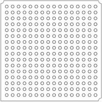
LFXP2-5E-5FTN256I Lattice, LFXP2-5E-5FTN256I Datasheet - Page 128

LFXP2-5E-5FTN256I
Manufacturer Part Number
LFXP2-5E-5FTN256I
Description
FPGA - Field Programmable Gate Array 5K LUTs 172 I/O Inst on DSP 1.2V -5 Spd
Manufacturer
Lattice
Datasheet
1.LFXP2-8E-5FTN256I.pdf
(341 pages)
Specifications of LFXP2-5E-5FTN256I
Number Of Macrocells
5000
Number Of Programmable I/os
172
Data Ram Size
169984
Supply Voltage (max)
1.26 V
Maximum Operating Temperature
+ 100 C
Minimum Operating Temperature
- 40 C
Mounting Style
SMD/SMT
Supply Voltage (min)
1.14 V
Package / Case
FTBGA-256
Number Of Logic Elements/cells
*
Number Of Labs/clbs
*
Total Ram Bits
169984
Number Of I /o
172
Number Of Gates
-
Voltage - Supply
1.14 V ~ 1.26 V
Mounting Type
*
Operating Temperature
-40°C ~ 100°C
Lead Free Status / RoHS Status
Lead free / RoHS Compliant
Available stocks
Company
Part Number
Manufacturer
Quantity
Price
Company:
Part Number:
LFXP2-5E-5FTN256I
Manufacturer:
Lattice
Quantity:
135
Company:
Part Number:
LFXP2-5E-5FTN256I
Manufacturer:
LATTICE
Quantity:
23
Company:
Part Number:
LFXP2-5E-5FTN256I
Manufacturer:
Lattice Semiconductor Corporation
Quantity:
10 000
Part Number:
LFXP2-5E-5FTN256I
Manufacturer:
LATTICE
Quantity:
20 000
- Current page: 128 of 341
- Download datasheet (10Mb)
LatticeXP2 sysCLOCK PLL
Lattice Semiconductor
Design and Usage Guide
Figure 9-5. RST Input Timing Diagram
t
RST
PLL_RST
t
LOCK
LOCK
RSTK Input
RSTK is the reset input for the K-Divider. This K-Divider reset is used to synchronize the K-Divider output clock to
the input clock. LatticeXP2 has an optional gearbox in the I/O cell for both outputs and inputs. The K-Divider reset
is useful for the gearbox implementation. RSTK is active high.
CLKFB Input
The feedback signal to the PLL, which is fed through the feedback divider, can be derived from the Primary Clock
net (CLKOP), a preferred pin, directly from the CLKOP divider or from general routing. External feedback allows the
designer to compensate for board-level clock alignment.
CLKOP Output
The sysCLOCK PLL main clock output, CLKOP, is a signal available for selection as a primary clock. This clock sig-
nal is available at the CLK_OUT pin.
CLKOS Output with Phase and Duty Cycle Select
The sysCLOCK PLL auxiliary clock output, CLKOS, is a signal available for selection as a primary clock. The
CLKOS is used when phase shift and/or duty cycle adjustment is desired. The programmable phase shift allows for
different phase in increments of 22.5°. The duty select feature provides duty select in 1/16th of the clock period.
This feature is also supported in Dynamic Control Mode.
CLKOK Output with Lower Frequency
The CLKOK is used when a lower frequency is desired. It is a signal available for selection as a primary clock.
CLKOK2 Output
This extra clock is provided for SPI4.2 application. The 420 MHz CLKOP clock is divided by 3, producing 140 MHz.
The clock can also be used for any applications where CLKOP-divided-by-3 is required.
LOCK Output
The LOCK output provides information about the status of the PLL. After the device is powered up and the input
clock is valid, the PLL will achieve lock within the specified lock time. Once lock is achieved, the PLL lock signal will
be asserted. If, during operation, the input clock or feedback signals to the PLL become invalid, the PLL will lose
lock. However, when the input clock completely stops, the LOCK output will remain in its last state, since it is inter-
nally registered by this clock. It is recommended to assert PLL RST to re-synchronize the PLL to the reference
®
clock. The LOCK signal is available to the FPGA routing to implement generation of RST. ModelSim
simulation
models take two to four reference clock cycles from RST release to LOCK high.
Dynamic Phase and Dynamic Duty Cycle Adjustment
The DPHASE[3:0] port is used with the Dynamic Phase Adjustment feature to allow the user to connect a control
signal to the PLL. The DDUTY[3:0] port is used with the Dynamic Duty Adjustment feature to allow the user to con-
nect a control signal to the PLL. The DPHASE and DDUTY ports are listed in Table 9-3.
The Dynamic Phase and Dynamic Duty Cycle Adjustment features will be discussed in more detail in later sections
of this document.
9-6
Related parts for LFXP2-5E-5FTN256I
Image
Part Number
Description
Manufacturer
Datasheet
Request
R

Part Number:
Description:
FPGA - Field Programmable Gate Array 5K LUTs 146I/O Inst- on DSP 1.2V -5 Spd
Manufacturer:
Lattice
Datasheet:

Part Number:
Description:
FPGA - Field Programmable Gate Array 5K LUTs 172I/O Inst- on DSP 1.2V -5 Spd
Manufacturer:
Lattice
Datasheet:

Part Number:
Description:
FPGA - Field Programmable Gate Array 5K LUTs 100 I/O Inst on DSP 1.2V -5 Spd
Manufacturer:
Lattice
Datasheet:

Part Number:
Description:
FPGA - Field Programmable Gate Array 5K LUTs 100I/O Inst- on DSP 1.2V -5 Spd
Manufacturer:
Lattice
Datasheet:
Part Number:
Description:
FPGA LatticeXP2 Family 5000 Cells Flash Technology 1.2V 256-Pin FTBGA
Manufacturer:
LATTICE SEMICONDUCTOR
Datasheet:
Part Number:
Description:
FPGA LatticeXP2 Family 5000 Cells Flash Technology 1.2V 256-Pin FTBGA
Manufacturer:
LATTICE SEMICONDUCTOR
Datasheet:

Part Number:
Description:
IC DSP 5KLUTS 100I/O 144TQFP
Manufacturer:
Lattice
Datasheet:

Part Number:
Description:
IC DSP 5KLUTS 86I/O 132CSBGA
Manufacturer:
Lattice
Datasheet:

Part Number:
Description:
IC DSP 5KLUTS 86I/O 132CSBGA
Manufacturer:
Lattice
Datasheet:

Part Number:
Description:
IC DSP 5KLUTS 146I/O 208PQFP
Manufacturer:
Lattice
Datasheet:

Part Number:
Description:
IC DSP 5KLUTS 146I/O 208PQFP
Manufacturer:
Lattice
Datasheet:

Part Number:
Description:
IC DSP 5KLUTS 172I/O 256FTBGA
Manufacturer:
Lattice
Datasheet:

Part Number:
Description:
IC FPGA 5KLUTS 86I/O 132-BGA
Manufacturer:
Lattice
Datasheet:

Part Number:
Description:
IC FPGA 5KLUTS 86I/O 132-BGA
Manufacturer:
Lattice
Datasheet:

Part Number:
Description:
IC FPGA 5KLUTS 86I/O 132-BGA
Manufacturer:
Lattice
Datasheet:


