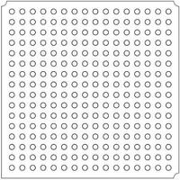
LFXP2-5E-5FTN256I Lattice, LFXP2-5E-5FTN256I Datasheet - Page 192

LFXP2-5E-5FTN256I
Manufacturer Part Number
LFXP2-5E-5FTN256I
Description
FPGA - Field Programmable Gate Array 5K LUTs 172 I/O Inst on DSP 1.2V -5 Spd
Manufacturer
Lattice
Datasheet
1.LFXP2-8E-5FTN256I.pdf
(341 pages)
Specifications of LFXP2-5E-5FTN256I
Number Of Macrocells
5000
Number Of Programmable I/os
172
Data Ram Size
169984
Supply Voltage (max)
1.26 V
Maximum Operating Temperature
+ 100 C
Minimum Operating Temperature
- 40 C
Mounting Style
SMD/SMT
Supply Voltage (min)
1.14 V
Package / Case
FTBGA-256
Number Of Logic Elements/cells
*
Number Of Labs/clbs
*
Total Ram Bits
169984
Number Of I /o
172
Number Of Gates
-
Voltage - Supply
1.14 V ~ 1.26 V
Mounting Type
*
Operating Temperature
-40°C ~ 100°C
Lead Free Status / RoHS Status
Lead free / RoHS Compliant
Available stocks
Company
Part Number
Manufacturer
Quantity
Price
Company:
Part Number:
LFXP2-5E-5FTN256I
Manufacturer:
Lattice
Quantity:
135
Company:
Part Number:
LFXP2-5E-5FTN256I
Manufacturer:
LATTICE
Quantity:
23
Company:
Part Number:
LFXP2-5E-5FTN256I
Manufacturer:
Lattice Semiconductor Corporation
Quantity:
10 000
Part Number:
LFXP2-5E-5FTN256I
Manufacturer:
LATTICE
Quantity:
20 000
- Current page: 192 of 341
- Download datasheet (10Mb)
Lattice Semiconductor
Table 10-19. Timing Specifications
Figure 10-49. Generic Timing Diagram
Programming via the SPI Interface
Since the SSPIA module is an internal module, I/Os can be treated as I/Os of any other soft module. Therefore,
they can be routed to other internal modules, or they can go out to I/O pads. The recommended routing is to the
sysCONFIG port pins.
Table 10-20. Usage Of Commands
CSSPISN
CCLK
SISPI
SO
READ_TAG
PROGRAM_TAG
ERASE_TAG
1. Data bytes are shifted with most significant bit first.
2. Byte 1-3 are dummy clocks to provide extra timing for the device to execute the command. The data presented at the SI pin
Command Name
f
t
t
t
t
t
t
t
t
t
t
t
Note: If the READ_TAG command is issued without first loading the WRITE_EN command, the device will need extra time,
up to 20µs maximum, to transfer the data from TAG Flash to the data-shift register.
MAXSPI
RF
CSCCLK
SOCDO
SCS
SCSS
SCSH
STSU
STH
STVO
STCO
SDIS
during these dummy clocks can be any value and do not have to be 0x00 as shown.
Symbol
0
t
Shifting Clocks
t
SCSS
Slave SPI CCLK Clock Frequency
Clock and Data Input Rise and Fall Time
Slave SPI CCLK Clock High Time
Slave SPI CCLK Clock Low Time
CSSPIN High Time
CSSPIN Setup Time
CSSPIN Hold Time
Slave SPI Data In Setup Time
Slave SPI Data In Hold Time
Slave SPI Output Valid (after WRITE_EN)
Slave SPI Output Valid (without WRITE_EN)(1)
Slave SPI Output Hold Time
Slave SPI Output Disable Time
STSU
Command
OPCODE
8 Command
0x4E
0x8E
0x0E
t
STH
7 8
Bytes 1-3
Dummy
Dummy
Dummy
t
STSU
Parameter
3-Byte Dummy
1, 2
HI-Z
t
10-42
Data
CSCLK
t
Out
STVO
In
3µs min.
1ms min., 25ms max.
100ms min., 1000ms max. Erase TAG memory
31 32
0 1 2
Delay Time
Byte Bounded Data Out
LatticeXP2 Memory Usage Guide
Data Shifting Clocks
t
STCO
t
SOCDO
Min
20
20
25
25
25
5
5
3
0
Read TAG memory
Program TAG memory
Max
100
25
20
20
20
(n-1) th
Description
n-1
Units
MHz
t
µs
SCS
ns
ns
ns
ns
ns
ns
ns
ns
ns
ns
ns
HI-Z
t
t
SCSH
SDIS
Related parts for LFXP2-5E-5FTN256I
Image
Part Number
Description
Manufacturer
Datasheet
Request
R

Part Number:
Description:
FPGA - Field Programmable Gate Array 5K LUTs 146I/O Inst- on DSP 1.2V -5 Spd
Manufacturer:
Lattice
Datasheet:

Part Number:
Description:
FPGA - Field Programmable Gate Array 5K LUTs 172I/O Inst- on DSP 1.2V -5 Spd
Manufacturer:
Lattice
Datasheet:

Part Number:
Description:
FPGA - Field Programmable Gate Array 5K LUTs 100 I/O Inst on DSP 1.2V -5 Spd
Manufacturer:
Lattice
Datasheet:

Part Number:
Description:
FPGA - Field Programmable Gate Array 5K LUTs 100I/O Inst- on DSP 1.2V -5 Spd
Manufacturer:
Lattice
Datasheet:
Part Number:
Description:
FPGA LatticeXP2 Family 5000 Cells Flash Technology 1.2V 256-Pin FTBGA
Manufacturer:
LATTICE SEMICONDUCTOR
Datasheet:
Part Number:
Description:
FPGA LatticeXP2 Family 5000 Cells Flash Technology 1.2V 256-Pin FTBGA
Manufacturer:
LATTICE SEMICONDUCTOR
Datasheet:

Part Number:
Description:
IC DSP 5KLUTS 100I/O 144TQFP
Manufacturer:
Lattice
Datasheet:

Part Number:
Description:
IC DSP 5KLUTS 86I/O 132CSBGA
Manufacturer:
Lattice
Datasheet:

Part Number:
Description:
IC DSP 5KLUTS 86I/O 132CSBGA
Manufacturer:
Lattice
Datasheet:

Part Number:
Description:
IC DSP 5KLUTS 146I/O 208PQFP
Manufacturer:
Lattice
Datasheet:

Part Number:
Description:
IC DSP 5KLUTS 146I/O 208PQFP
Manufacturer:
Lattice
Datasheet:

Part Number:
Description:
IC DSP 5KLUTS 172I/O 256FTBGA
Manufacturer:
Lattice
Datasheet:

Part Number:
Description:
IC FPGA 5KLUTS 86I/O 132-BGA
Manufacturer:
Lattice
Datasheet:

Part Number:
Description:
IC FPGA 5KLUTS 86I/O 132-BGA
Manufacturer:
Lattice
Datasheet:

Part Number:
Description:
IC FPGA 5KLUTS 86I/O 132-BGA
Manufacturer:
Lattice
Datasheet:


