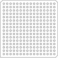
LFXP2-5E-5FTN256I Lattice, LFXP2-5E-5FTN256I Datasheet - Page 242

LFXP2-5E-5FTN256I
Manufacturer Part Number
LFXP2-5E-5FTN256I
Description
FPGA - Field Programmable Gate Array 5K LUTs 172 I/O Inst on DSP 1.2V -5 Spd
Manufacturer
Lattice
Datasheet
1.LFXP2-8E-5FTN256I.pdf
(341 pages)
Specifications of LFXP2-5E-5FTN256I
Number Of Macrocells
5000
Number Of Programmable I/os
172
Data Ram Size
169984
Supply Voltage (max)
1.26 V
Maximum Operating Temperature
+ 100 C
Minimum Operating Temperature
- 40 C
Mounting Style
SMD/SMT
Supply Voltage (min)
1.14 V
Package / Case
FTBGA-256
Number Of Logic Elements/cells
*
Number Of Labs/clbs
*
Total Ram Bits
169984
Number Of I /o
172
Number Of Gates
-
Voltage - Supply
1.14 V ~ 1.26 V
Mounting Type
*
Operating Temperature
-40°C ~ 100°C
Lead Free Status / RoHS Status
Lead free / RoHS Compliant
Available stocks
Company
Part Number
Manufacturer
Quantity
Price
Company:
Part Number:
LFXP2-5E-5FTN256I
Manufacturer:
Lattice
Quantity:
135
Company:
Part Number:
LFXP2-5E-5FTN256I
Manufacturer:
LATTICE
Quantity:
23
Company:
Part Number:
LFXP2-5E-5FTN256I
Manufacturer:
Lattice Semiconductor Corporation
Quantity:
10 000
Part Number:
LFXP2-5E-5FTN256I
Manufacturer:
LATTICE
Quantity:
20 000
- Current page: 242 of 341
- Download datasheet (10Mb)
Lattice Semiconductor
Figure 11-46. Configuration Tab for DDR_MEM
The user can change the Mode parameter to choose either the DDR or DDR2 interface. The other configuration
parameters will change according to the Mode selected. The Number of DQS parameter determines the number of
DDR interfaces. The software will assume there are eight data bits for every DQS. The user can also choose the
frequency of operation and the DDR DLL will be configured to this frequency.
The user has an option to enable the clock enable and tristate enables for the DDR registers. It is recommend that
the Lock/Jitter be enabled if the DDR interface is running at 150MHz or higher.
The parameters available depend on the mode selected. Tables 11-13 and 11-14 describe all user parameters in
the IPexpress GUI and their usage for modes DDR and DDR2.
Table 11-13. User Parameters in the IPexpress GUI when in DDR Mode
I/O Buffer Configuration
Data Width
Number of DQS
Frequency of DQS
Lock/Jitter Sensitivity
LSR for DDR Input Register
Create Clock Enable for DDR
Input Register
Tri-state Enable for DDR
Output Registers
DDR Tristate enable for the
DQS output
User Parameters
LSR Control
I/O Standard used for the Interface. This will
also depend on the Mode selected.
Width of the Data bus
Number of DQS will determine the number of
DQS Groups
DDR Interface Frequency. This is also input to
the DDR DLL. The values will depend on the
mode selected.
DLL Sensitivity to Jitter
Create Clock enable inputs to the block
Creates Tri-state control for the DDR data output
registers.
Creates Tristate control for DQS output
Description
11-38
LatticeXP2 High-Speed I/O Interface
100MHz, 133MHz,
166MHz, 200MHz
Values/Range
RESET, SET
SSTL25_I,
SSTL25_II
High, Low
1, 2, 4, 8
On/Off
On/Off
On/Off
8-64
SSTL25_I
200MHz
Default
RESET
High
Off
On
On
8
1
Related parts for LFXP2-5E-5FTN256I
Image
Part Number
Description
Manufacturer
Datasheet
Request
R

Part Number:
Description:
FPGA - Field Programmable Gate Array 5K LUTs 146I/O Inst- on DSP 1.2V -5 Spd
Manufacturer:
Lattice
Datasheet:

Part Number:
Description:
FPGA - Field Programmable Gate Array 5K LUTs 172I/O Inst- on DSP 1.2V -5 Spd
Manufacturer:
Lattice
Datasheet:

Part Number:
Description:
FPGA - Field Programmable Gate Array 5K LUTs 100 I/O Inst on DSP 1.2V -5 Spd
Manufacturer:
Lattice
Datasheet:

Part Number:
Description:
FPGA - Field Programmable Gate Array 5K LUTs 100I/O Inst- on DSP 1.2V -5 Spd
Manufacturer:
Lattice
Datasheet:
Part Number:
Description:
FPGA LatticeXP2 Family 5000 Cells Flash Technology 1.2V 256-Pin FTBGA
Manufacturer:
LATTICE SEMICONDUCTOR
Datasheet:
Part Number:
Description:
FPGA LatticeXP2 Family 5000 Cells Flash Technology 1.2V 256-Pin FTBGA
Manufacturer:
LATTICE SEMICONDUCTOR
Datasheet:

Part Number:
Description:
IC DSP 5KLUTS 100I/O 144TQFP
Manufacturer:
Lattice
Datasheet:

Part Number:
Description:
IC DSP 5KLUTS 86I/O 132CSBGA
Manufacturer:
Lattice
Datasheet:

Part Number:
Description:
IC DSP 5KLUTS 86I/O 132CSBGA
Manufacturer:
Lattice
Datasheet:

Part Number:
Description:
IC DSP 5KLUTS 146I/O 208PQFP
Manufacturer:
Lattice
Datasheet:

Part Number:
Description:
IC DSP 5KLUTS 146I/O 208PQFP
Manufacturer:
Lattice
Datasheet:

Part Number:
Description:
IC DSP 5KLUTS 172I/O 256FTBGA
Manufacturer:
Lattice
Datasheet:

Part Number:
Description:
IC FPGA 5KLUTS 86I/O 132-BGA
Manufacturer:
Lattice
Datasheet:

Part Number:
Description:
IC FPGA 5KLUTS 86I/O 132-BGA
Manufacturer:
Lattice
Datasheet:

Part Number:
Description:
IC FPGA 5KLUTS 86I/O 132-BGA
Manufacturer:
Lattice
Datasheet:


