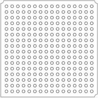
LFXP2-5E-5FTN256I Lattice, LFXP2-5E-5FTN256I Datasheet - Page 209

LFXP2-5E-5FTN256I
Manufacturer Part Number
LFXP2-5E-5FTN256I
Description
FPGA - Field Programmable Gate Array 5K LUTs 172 I/O Inst on DSP 1.2V -5 Spd
Manufacturer
Lattice
Datasheet
1.LFXP2-8E-5FTN256I.pdf
(341 pages)
Specifications of LFXP2-5E-5FTN256I
Number Of Macrocells
5000
Number Of Programmable I/os
172
Data Ram Size
169984
Supply Voltage (max)
1.26 V
Maximum Operating Temperature
+ 100 C
Minimum Operating Temperature
- 40 C
Mounting Style
SMD/SMT
Supply Voltage (min)
1.14 V
Package / Case
FTBGA-256
Number Of Logic Elements/cells
*
Number Of Labs/clbs
*
Total Ram Bits
169984
Number Of I /o
172
Number Of Gates
-
Voltage - Supply
1.14 V ~ 1.26 V
Mounting Type
*
Operating Temperature
-40°C ~ 100°C
Lead Free Status / RoHS Status
Lead free / RoHS Compliant
Available stocks
Company
Part Number
Manufacturer
Quantity
Price
Company:
Part Number:
LFXP2-5E-5FTN256I
Manufacturer:
Lattice
Quantity:
135
Company:
Part Number:
LFXP2-5E-5FTN256I
Manufacturer:
LATTICE
Quantity:
23
Company:
Part Number:
LFXP2-5E-5FTN256I
Manufacturer:
Lattice Semiconductor Corporation
Quantity:
10 000
Part Number:
LFXP2-5E-5FTN256I
Manufacturer:
LATTICE
Quantity:
20 000
- Current page: 209 of 341
- Download datasheet (10Mb)
Lattice Semiconductor
DQSDLL Configuration: By default, this DLL will generate a 90-degree phase shift for the DQS strobe based on
the frequency of the input reference clock to the DLL. The user can control the sensitivity to jitter by using the
LOCK_SENSITIVITY attribute. This configuration bit can be programmed to be either “HIGH” or “LOW”.
The DLL Lock Detect circuit has two modes of operation controlled by the LOCK_SENSITIVITY bit, which selects
more or less sensitivity to jitter. If this DLL is operated at or above 150 MHz, it is recommended that the
LOCK_SENSITIVITY bit be programmed “HIGH” (more sensitive). When running at or below 100 MHz, it is recom-
mended that the bit be programmed “LOW” (more tolerant). For 133 MHz, the LOCK_SENSITIVITY bit can go
either way.
DQSBUFC
This primitive implements the DQS delay and the DQS transition detector logic. Figure 11-7 shows the primitive
symbol.
Figure 11-7. DQSBUFC Symbol
The DQSBUFC is composed of the DQS Delay, the DQS Transition Detect and the DQSXFER block as shown in
Figure 11-8. This block inputs the DQS and delays it by 90 degrees. It also generates the DDR Clock Polarity and
the DQSXFER signal. The preamble detect (PRMBDET) signal is generated from the DQSI input using a voltage
divider circuit.
DQSI
CLK
READ
DQSDEL
XCLK
DQSBUFC
11-5
DDRCLKPOL
DATAVALID
PRMBDET
DQSXFER
DQSO
DQSC
LatticeXP2 High-Speed I/O Interface
Related parts for LFXP2-5E-5FTN256I
Image
Part Number
Description
Manufacturer
Datasheet
Request
R

Part Number:
Description:
FPGA - Field Programmable Gate Array 5K LUTs 146I/O Inst- on DSP 1.2V -5 Spd
Manufacturer:
Lattice
Datasheet:

Part Number:
Description:
FPGA - Field Programmable Gate Array 5K LUTs 172I/O Inst- on DSP 1.2V -5 Spd
Manufacturer:
Lattice
Datasheet:

Part Number:
Description:
FPGA - Field Programmable Gate Array 5K LUTs 100 I/O Inst on DSP 1.2V -5 Spd
Manufacturer:
Lattice
Datasheet:

Part Number:
Description:
FPGA - Field Programmable Gate Array 5K LUTs 100I/O Inst- on DSP 1.2V -5 Spd
Manufacturer:
Lattice
Datasheet:
Part Number:
Description:
FPGA LatticeXP2 Family 5000 Cells Flash Technology 1.2V 256-Pin FTBGA
Manufacturer:
LATTICE SEMICONDUCTOR
Datasheet:
Part Number:
Description:
FPGA LatticeXP2 Family 5000 Cells Flash Technology 1.2V 256-Pin FTBGA
Manufacturer:
LATTICE SEMICONDUCTOR
Datasheet:

Part Number:
Description:
IC DSP 5KLUTS 100I/O 144TQFP
Manufacturer:
Lattice
Datasheet:

Part Number:
Description:
IC DSP 5KLUTS 86I/O 132CSBGA
Manufacturer:
Lattice
Datasheet:

Part Number:
Description:
IC DSP 5KLUTS 86I/O 132CSBGA
Manufacturer:
Lattice
Datasheet:

Part Number:
Description:
IC DSP 5KLUTS 146I/O 208PQFP
Manufacturer:
Lattice
Datasheet:

Part Number:
Description:
IC DSP 5KLUTS 146I/O 208PQFP
Manufacturer:
Lattice
Datasheet:

Part Number:
Description:
IC DSP 5KLUTS 172I/O 256FTBGA
Manufacturer:
Lattice
Datasheet:

Part Number:
Description:
IC FPGA 5KLUTS 86I/O 132-BGA
Manufacturer:
Lattice
Datasheet:

Part Number:
Description:
IC FPGA 5KLUTS 86I/O 132-BGA
Manufacturer:
Lattice
Datasheet:

Part Number:
Description:
IC FPGA 5KLUTS 86I/O 132-BGA
Manufacturer:
Lattice
Datasheet:


