HD64F2218UTF24 Renesas Electronics America, HD64F2218UTF24 Datasheet - Page 740
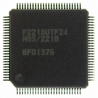
HD64F2218UTF24
Manufacturer Part Number
HD64F2218UTF24
Description
IC H8S MCU FLASH 128K 100-TQFP
Manufacturer
Renesas Electronics America
Series
H8® H8S/2200r
Specifications of HD64F2218UTF24
Core Processor
H8S/2000
Core Size
16-Bit
Speed
24MHz
Connectivity
SCI, SmartCard, USB
Peripherals
DMA, POR, PWM, WDT
Number Of I /o
69
Program Memory Size
128KB (128K x 8)
Program Memory Type
FLASH
Ram Size
12K x 8
Voltage - Supply (vcc/vdd)
2.7 V ~ 3.6 V
Data Converters
A/D 6x10b
Oscillator Type
Internal
Operating Temperature
-20°C ~ 75°C
Package / Case
100-TQFP, 100-VQFP
For Use With
3DK2218-SS - KIT DEV H8S/2218 WINDOWS SIDESHW
Lead Free Status / RoHS Status
Contains lead / RoHS non-compliant
Eeprom Size
-
Available stocks
Company
Part Number
Manufacturer
Quantity
Price

Part Number:
HD64F2218UTF24V
Manufacturer:
RENESAS/瑞萨
Quantity:
20 000


22.8
General Notice during Design for Printed Circuit Board: Measures for radiation noise caused
by the transient current in this LSI should be taken into consideration. The examples of the
measures are shown below.
• To use a multilayer printed circuit board which includes layers for Vcc and GND.
• To mount by-pass capacitors (approximately 0.1 μF) between the Vcc and GND (Vss) pins,
Characteristics of F-ZTAT and Masked ROM Versions: Though the F-ZTAT version and the
masked ROM version satisfy electrical characteristics described in this manual, the actual value of
electrical characteristics, operating margin, and noise margin may differ due to the differences of
production process, on-chip ROM, and layout patterning.
When the system has been evaluated with the F-ZTAT version, the equivalent evaluation should
be implemented to the masked ROM version when shifted to the masked ROM version.
Rev.7.00 Dec. 24, 2008 Page 684 of 698
REJ09B0074-0700
and the PLLVcc and PLLGND pins, of this LSI.
3. Block erase time (Shows the total period for which the E1-bit FLMCR1 is set. It does not
4. Maximum programming time value
5. Maximum erasure time value
6. Minimum times that guarantee all characteristics after programming. (The guaranteed
7. Reference value when the temperature is 25°C. (It is reference that reprogramming is
8. Data hold characteristics when reprogramming is performed within the range of
Usage Note
include the erase verification time.)
t
range is 1 to the minimum value.)
normally enabled up to this value.)
specifications including the minimum value.
E
(max.) = Wait time after E1 bit set (z) × maximum erasure count (N)
t
p
(max.) = Wait time after P1 bit set (z) × maximum programming count (N1 + N2)
= (Z0 + Z2) × 6 + Z1 × 994
Related parts for HD64F2218UTF24
Image
Part Number
Description
Manufacturer
Datasheet
Request
R

Part Number:
Description:
KIT STARTER FOR M16C/29
Manufacturer:
Renesas Electronics America
Datasheet:

Part Number:
Description:
KIT STARTER FOR R8C/2D
Manufacturer:
Renesas Electronics America
Datasheet:

Part Number:
Description:
R0K33062P STARTER KIT
Manufacturer:
Renesas Electronics America
Datasheet:

Part Number:
Description:
KIT STARTER FOR R8C/23 E8A
Manufacturer:
Renesas Electronics America
Datasheet:

Part Number:
Description:
KIT STARTER FOR R8C/25
Manufacturer:
Renesas Electronics America
Datasheet:

Part Number:
Description:
KIT STARTER H8S2456 SHARPE DSPLY
Manufacturer:
Renesas Electronics America
Datasheet:

Part Number:
Description:
KIT STARTER FOR R8C38C
Manufacturer:
Renesas Electronics America
Datasheet:

Part Number:
Description:
KIT STARTER FOR R8C35C
Manufacturer:
Renesas Electronics America
Datasheet:

Part Number:
Description:
KIT STARTER FOR R8CL3AC+LCD APPS
Manufacturer:
Renesas Electronics America
Datasheet:
Part Number:
Description:
KIT STARTER FOR RX610
Manufacturer:
Renesas Electronics America
Datasheet:

Part Number:
Description:
KIT STARTER FOR R32C/118
Manufacturer:
Renesas Electronics America
Datasheet:

Part Number:
Description:
KIT DEV RSK-R8C/26-29
Manufacturer:
Renesas Electronics America
Datasheet:

Part Number:
Description:
KIT STARTER FOR SH7124
Manufacturer:
Renesas Electronics America
Datasheet:

Part Number:
Description:
KIT STARTER FOR H8SX/1622
Manufacturer:
Renesas Electronics America
Datasheet:

Part Number:
Description:
KIT DEV FOR SH7203
Manufacturer:
Renesas Electronics America
Datasheet: