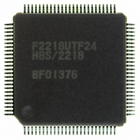
HD64F2218UTF24 Renesas Electronics America, HD64F2218UTF24 Datasheet - Page 45

HD64F2218UTF24
Manufacturer Part Number
HD64F2218UTF24
Description
IC H8S MCU FLASH 128K 100-TQFP
Manufacturer
Renesas Electronics America
Series
H8® H8S/2200r
Specifications of HD64F2218UTF24
Core Processor
H8S/2000
Core Size
16-Bit
Speed
24MHz
Connectivity
SCI, SmartCard, USB
Peripherals
DMA, POR, PWM, WDT
Number Of I /o
69
Program Memory Size
128KB (128K x 8)
Program Memory Type
FLASH
Ram Size
12K x 8
Voltage - Supply (vcc/vdd)
2.7 V ~ 3.6 V
Data Converters
A/D 6x10b
Oscillator Type
Internal
Operating Temperature
-20°C ~ 75°C
Package / Case
100-TQFP, 100-VQFP
For Use With
3DK2218-SS - KIT DEV H8S/2218 WINDOWS SIDESHW
Lead Free Status / RoHS Status
Contains lead / RoHS non-compliant
Eeprom Size
-
Available stocks
Company
Part Number
Manufacturer
Quantity
Price
Part Number:
HD64F2218UTF24V
Manufacturer:
RENESAS/瑞萨
Quantity:
20 000
- Current page: 45 of 758
- Download datasheet (5Mb)
Figure 12.35 Clock Halt and Restart Procedure .......................................................................... 437
Figure 12.36 Example of Communication Using the SCI Select Function ................................. 438
Figure 12.37 Example of Communication Using the SCI Select Function ................................. 439
Figure 12.38 Example of Clocked Synchronous Transmission by DMAC ................................. 442
Figure 12.39 Sample Flowchart for Mode Transition during Transmission................................ 444
Figure 12.40 Port Pin State of Asynchronous Transmission Using Internal Clock ..................... 444
Figure 12.41 Port Pin State of Synchronous Transmission Using Internal Clock ....................... 445
Figure 12.42 Sample Flowchart for Mode Transition during Reception ..................................... 446
Figure 12.43 Operation when Switching from SCK Pin Function to Port Pin Function ............. 447
Figure 12.44 Operation when Switching from SCK Pin Function to Port Pin Function
Section 13 Boundary Scan Function
Figure 13.1 Block Diagram of Boundary Scan Function........................................................... 450
Figure 13.2 Boundary Scan Register Configuration.................................................................. 455
Figure 13.3 TAP Controller Status Transition........................................................................... 462
Figure 13.4 Recommended Reset Signal Design....................................................................... 463
Figure 13.5 Serial Data Input/Output ........................................................................................ 463
Section 14 Universal Serial Bus (USB)
Figure 14.1 Block Diagram of USB .......................................................................................... 466
Figure 14.2 USB Initialization................................................................................................... 497
Figure 14.3 USB Cable Connection
Figure 14.4 USB Cable Connection
Figure 14.5 USB Cable Disconnection
Figure 14.6 USB Cable Disconnection
Figure 14.7 Example Flowchart of Suspend and Resume Operations....................................... 502
Figure 14.8 Example Flowchart of Suspend and Resume Interrupt Processing ........................ 503
Figure 14.9 Example Flowchart of Suspend and Remote-Wakeup Operations......................... 504
Figure 14.10 Example Flowchart of Remote-Wakeup Interrupt Processing ............................... 505
Figure 14.11 Control Transfer Stage Configuration .................................................................... 506
Figure 14.12 Setup Stage Operation ............................................................................................ 507
Figure 14.13 Data Stage Operation (Control-In) ......................................................................... 508
Figure 14.14 Data Stage Operation (Control-Out)....................................................................... 509
Figure 14.15 Status Stage Operation (Control-In) ....................................................................... 510
Figure 14.16 Status Stage Operation (Control-Out) .................................................................... 511
Figure 14.17 EP3 Interrupt-In Transfer Operation ...................................................................... 512
(Example of Preventing Low-Level Output).......................................................... 448
(When USB Module Stop or Power-Down Mode Is not Used).............................. 498
(When USB Module Stop or Power-Down Mode Is Used).................................... 499
(When USB Module Stop or Power-Down Mode Is not Used).............................. 500
(When USB Module Stop or Power-Down Mode Is Used).................................... 501
Rev.7.00 Dec. 24, 2008 Page xliii of liv
REJ09B0074-0700
Related parts for HD64F2218UTF24
Image
Part Number
Description
Manufacturer
Datasheet
Request
R

Part Number:
Description:
KIT STARTER FOR M16C/29
Manufacturer:
Renesas Electronics America
Datasheet:

Part Number:
Description:
KIT STARTER FOR R8C/2D
Manufacturer:
Renesas Electronics America
Datasheet:

Part Number:
Description:
R0K33062P STARTER KIT
Manufacturer:
Renesas Electronics America
Datasheet:

Part Number:
Description:
KIT STARTER FOR R8C/23 E8A
Manufacturer:
Renesas Electronics America
Datasheet:

Part Number:
Description:
KIT STARTER FOR R8C/25
Manufacturer:
Renesas Electronics America
Datasheet:

Part Number:
Description:
KIT STARTER H8S2456 SHARPE DSPLY
Manufacturer:
Renesas Electronics America
Datasheet:

Part Number:
Description:
KIT STARTER FOR R8C38C
Manufacturer:
Renesas Electronics America
Datasheet:

Part Number:
Description:
KIT STARTER FOR R8C35C
Manufacturer:
Renesas Electronics America
Datasheet:

Part Number:
Description:
KIT STARTER FOR R8CL3AC+LCD APPS
Manufacturer:
Renesas Electronics America
Datasheet:

Part Number:
Description:
KIT STARTER FOR RX610
Manufacturer:
Renesas Electronics America
Datasheet:

Part Number:
Description:
KIT STARTER FOR R32C/118
Manufacturer:
Renesas Electronics America
Datasheet:

Part Number:
Description:
KIT DEV RSK-R8C/26-29
Manufacturer:
Renesas Electronics America
Datasheet:

Part Number:
Description:
KIT STARTER FOR SH7124
Manufacturer:
Renesas Electronics America
Datasheet:

Part Number:
Description:
KIT STARTER FOR H8SX/1622
Manufacturer:
Renesas Electronics America
Datasheet:

Part Number:
Description:
KIT DEV FOR SH7203
Manufacturer:
Renesas Electronics America
Datasheet:


