HD64F2218UTF24 Renesas Electronics America, HD64F2218UTF24 Datasheet - Page 34
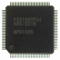
HD64F2218UTF24
Manufacturer Part Number
HD64F2218UTF24
Description
IC H8S MCU FLASH 128K 100-TQFP
Manufacturer
Renesas Electronics America
Series
H8® H8S/2200r
Specifications of HD64F2218UTF24
Core Processor
H8S/2000
Core Size
16-Bit
Speed
24MHz
Connectivity
SCI, SmartCard, USB
Peripherals
DMA, POR, PWM, WDT
Number Of I /o
69
Program Memory Size
128KB (128K x 8)
Program Memory Type
FLASH
Ram Size
12K x 8
Voltage - Supply (vcc/vdd)
2.7 V ~ 3.6 V
Data Converters
A/D 6x10b
Oscillator Type
Internal
Operating Temperature
-20°C ~ 75°C
Package / Case
100-TQFP, 100-VQFP
For Use With
3DK2218-SS - KIT DEV H8S/2218 WINDOWS SIDESHW
Lead Free Status / RoHS Status
Contains lead / RoHS non-compliant
Eeprom Size
-
Available stocks
Company
Part Number
Manufacturer
Quantity
Price

Part Number:
HD64F2218UTF24V
Manufacturer:
RENESAS/瑞萨
Quantity:
20 000


15.2 Input/Output Pins .............................................................................................................. 537
15.3 Register Descriptions......................................................................................................... 537
15.4 Interface to Bus Master ..................................................................................................... 541
15.5 Operation ........................................................................................................................... 542
15.6 Interrupts ........................................................................................................................... 546
15.7 A/D Conversion Precision Definitions .............................................................................. 546
15.8 Usage Notes....................................................................................................................... 548
Section 16 RAM
Section 17 Flash Memory (F-ZTAT Version)
17.1 Features ............................................................................................................................. 553
17.2 Mode Transitions............................................................................................................... 555
17.3 Block Configuration .......................................................................................................... 558
17.4 Input/Output Pins .............................................................................................................. 561
17.5 Register Descriptions......................................................................................................... 561
17.6 On-Board Programming Modes ........................................................................................ 567
17.7 Flash Memory Emulation in RAM.................................................................................... 577
17.8 Flash Memory Programming/Erasing................................................................................ 579
Rev.7.00 Dec. 24, 2008 Page xxxii of liv
REJ09B0074-0700
15.3.1 A/D Data Registers A to D (ADDRA to ADDRD).............................................. 538
15.3.2 A/D Control/Status Register (ADCSR)................................................................ 538
15.3.3 A/D Control Register (ADCR)............................................................................. 540
15.5.1 Single Mode ......................................................................................................... 542
15.5.2 Scan Mode............................................................................................................ 543
15.5.3 Input Sampling and A/D Conversion Time .......................................................... 544
15.5.4 External Trigger Input Timing ............................................................................. 545
15.8.1 Module Stop Mode Setting................................................................................... 548
15.8.2 Permissible Signal Source Impedance.................................................................. 548
15.8.3 Influences on Absolute Precision ......................................................................... 548
15.8.4 Range of Analog Power Supply and Other Pin Settings ...................................... 549
15.8.5 Notes on Board Design......................................................................................... 549
17.5.1 Flash Memory Control Register 1 (FLMCR1) ..................................................... 562
17.5.2 Flash Memory Control Register 2 (FLMCR2) ..................................................... 563
17.5.3 Erase Block Register 1 (EBR1)............................................................................ 564
17.5.4 Erase Block Register 2 (EBR2)............................................................................ 564
17.5.5 RAM Emulation Register (RAMER) ................................................................... 565
17.5.6 Serial Control Register X (SCRX) ....................................................................... 566
17.6.1 SCI Boot Mode (HD64F2218, HD64F2212, and HD64F2211)........................... 567
17.6.2 USB Boot Mode (HD64F2218U, HD64F2212U, and HD64F2211U)................. 571
17.6.3 Programming/Erasing in User Program Mode ..................................................... 576
17.8.1 Program/Program-Verify...................................................................................... 579
................................................................................................................... 551
............................................................. 553
Related parts for HD64F2218UTF24
Image
Part Number
Description
Manufacturer
Datasheet
Request
R

Part Number:
Description:
KIT STARTER FOR M16C/29
Manufacturer:
Renesas Electronics America
Datasheet:

Part Number:
Description:
KIT STARTER FOR R8C/2D
Manufacturer:
Renesas Electronics America
Datasheet:

Part Number:
Description:
R0K33062P STARTER KIT
Manufacturer:
Renesas Electronics America
Datasheet:

Part Number:
Description:
KIT STARTER FOR R8C/23 E8A
Manufacturer:
Renesas Electronics America
Datasheet:

Part Number:
Description:
KIT STARTER FOR R8C/25
Manufacturer:
Renesas Electronics America
Datasheet:

Part Number:
Description:
KIT STARTER H8S2456 SHARPE DSPLY
Manufacturer:
Renesas Electronics America
Datasheet:

Part Number:
Description:
KIT STARTER FOR R8C38C
Manufacturer:
Renesas Electronics America
Datasheet:

Part Number:
Description:
KIT STARTER FOR R8C35C
Manufacturer:
Renesas Electronics America
Datasheet:

Part Number:
Description:
KIT STARTER FOR R8CL3AC+LCD APPS
Manufacturer:
Renesas Electronics America
Datasheet:
Part Number:
Description:
KIT STARTER FOR RX610
Manufacturer:
Renesas Electronics America
Datasheet:

Part Number:
Description:
KIT STARTER FOR R32C/118
Manufacturer:
Renesas Electronics America
Datasheet:

Part Number:
Description:
KIT DEV RSK-R8C/26-29
Manufacturer:
Renesas Electronics America
Datasheet:

Part Number:
Description:
KIT STARTER FOR SH7124
Manufacturer:
Renesas Electronics America
Datasheet:

Part Number:
Description:
KIT STARTER FOR H8SX/1622
Manufacturer:
Renesas Electronics America
Datasheet:

Part Number:
Description:
KIT DEV FOR SH7203
Manufacturer:
Renesas Electronics America
Datasheet: