HD64F2218UTF24 Renesas Electronics America, HD64F2218UTF24 Datasheet - Page 205
HD64F2218UTF24
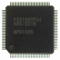
Manufacturer Part Number
HD64F2218UTF24
Description
IC H8S MCU FLASH 128K 100-TQFP
Manufacturer
Renesas Electronics America
Series
H8® H8S/2200r
Specifications of HD64F2218UTF24
Core Processor
H8S/2000
Core Size
16-Bit
Speed
24MHz
Connectivity
SCI, SmartCard, USB
Peripherals
DMA, POR, PWM, WDT
Number Of I /o
69
Program Memory Size
128KB (128K x 8)
Program Memory Type
FLASH
Ram Size
12K x 8
Voltage - Supply (vcc/vdd)
2.7 V ~ 3.6 V
Data Converters
A/D 6x10b
Oscillator Type
Internal
Operating Temperature
-20°C ~ 75°C
Package / Case
100-TQFP, 100-VQFP
For Use With
3DK2218-SS - KIT DEV H8S/2218 WINDOWS SIDESHW
Lead Free Status / RoHS Status
Contains lead / RoHS non-compliant
Eeprom Size
-
Available stocks
Company
Part Number
Manufacturer
Quantity
Price

Part Number:
HD64F2218UTF24V
Manufacturer:
RENESAS/瑞萨
Quantity:
20 000


6.7.2
As with the basic bus interface, either program wait insertion or pin wait insertion using the WAIT
pin can be used in the initial cycle (full access) of the burst ROM interface. See section 6.6.4, Wait
Control.
Wait states cannot be inserted in a burst cycle.
6.8
When the H8S/2218 Group accesses external space, it can insert a 1-state idle cycle (T
bus cycles in the following two cases: (1) when read accesses between different areas occur
consecutively, and (2) when a write cycle occurs immediately after a read cycle. By inserting an
idle cycle it is possible, for example, to avoid data collisions between ROM, with a long output
floating time, and high-speed memory, I/O interfaces, and so on.
Consecutive Reads between Different Areas: If consecutive reads between different areas occur
while the ICIS1 bit in BCRH is set to 1, an idle cycle is inserted at the start of the second read
cycle.
Figure 6.22 shows an example of the operation in this case. In this example, bus cycle A is a read
cycle from ROM with a long output floating time, and bus cycle B is a read cycle from SRAM,
each being located in a different area. In (a), an idle cycle is not inserted, and a collision occurs in
cycle B between the read data from ROM and that from SRAM. In (b), an idle cycle is inserted,
and a data collision is prevented.
Wait Control
Idle Cycle
Rev.7.00 Dec. 24, 2008 Page 149 of 698
REJ09B0074-0700
I
) between
Related parts for HD64F2218UTF24
Image
Part Number
Description
Manufacturer
Datasheet
Request
R

Part Number:
Description:
KIT STARTER FOR M16C/29
Manufacturer:
Renesas Electronics America
Datasheet:

Part Number:
Description:
KIT STARTER FOR R8C/2D
Manufacturer:
Renesas Electronics America
Datasheet:

Part Number:
Description:
R0K33062P STARTER KIT
Manufacturer:
Renesas Electronics America
Datasheet:

Part Number:
Description:
KIT STARTER FOR R8C/23 E8A
Manufacturer:
Renesas Electronics America
Datasheet:

Part Number:
Description:
KIT STARTER FOR R8C/25
Manufacturer:
Renesas Electronics America
Datasheet:

Part Number:
Description:
KIT STARTER H8S2456 SHARPE DSPLY
Manufacturer:
Renesas Electronics America
Datasheet:

Part Number:
Description:
KIT STARTER FOR R8C38C
Manufacturer:
Renesas Electronics America
Datasheet:

Part Number:
Description:
KIT STARTER FOR R8C35C
Manufacturer:
Renesas Electronics America
Datasheet:

Part Number:
Description:
KIT STARTER FOR R8CL3AC+LCD APPS
Manufacturer:
Renesas Electronics America
Datasheet:
Part Number:
Description:
KIT STARTER FOR RX610
Manufacturer:
Renesas Electronics America
Datasheet:

Part Number:
Description:
KIT STARTER FOR R32C/118
Manufacturer:
Renesas Electronics America
Datasheet:

Part Number:
Description:
KIT DEV RSK-R8C/26-29
Manufacturer:
Renesas Electronics America
Datasheet:

Part Number:
Description:
KIT STARTER FOR SH7124
Manufacturer:
Renesas Electronics America
Datasheet:

Part Number:
Description:
KIT STARTER FOR H8SX/1622
Manufacturer:
Renesas Electronics America
Datasheet:

Part Number:
Description:
KIT DEV FOR SH7203
Manufacturer:
Renesas Electronics America
Datasheet: