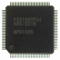
HD64F2218UTF24 Renesas Electronics America, HD64F2218UTF24 Datasheet - Page 486

HD64F2218UTF24
Manufacturer Part Number
HD64F2218UTF24
Description
IC H8S MCU FLASH 128K 100-TQFP
Manufacturer
Renesas Electronics America
Series
H8® H8S/2200r
Specifications of HD64F2218UTF24
Core Processor
H8S/2000
Core Size
16-Bit
Speed
24MHz
Connectivity
SCI, SmartCard, USB
Peripherals
DMA, POR, PWM, WDT
Number Of I /o
69
Program Memory Size
128KB (128K x 8)
Program Memory Type
FLASH
Ram Size
12K x 8
Voltage - Supply (vcc/vdd)
2.7 V ~ 3.6 V
Data Converters
A/D 6x10b
Oscillator Type
Internal
Operating Temperature
-20°C ~ 75°C
Package / Case
100-TQFP, 100-VQFP
For Use With
3DK2218-SS - KIT DEV H8S/2218 WINDOWS SIDESHW
Lead Free Status / RoHS Status
Contains lead / RoHS non-compliant
Eeprom Size
-
Available stocks
Company
Part Number
Manufacturer
Quantity
Price
Part Number:
HD64F2218UTF24V
Manufacturer:
RENESAS/瑞萨
Quantity:
20 000
- Current page: 486 of 758
- Download datasheet (5Mb)
12.7.5
In Smart Card interface mode an internal clock generated by the on-chip baud rate generator can
only be used as a transmission/reception clock. In this mode, the SCI operates on a basic clock
with a frequency of 32, 64, 372, or 256 times the transfer rate (fixed to 16 times in normal
asynchronous mode) as determined by bits BCP1 and BCP0. In reception, the SCI samples the
falling edge of the start bit using the basic clock, and performs internal synchronization. As shown
in figure 12.28, by sampling receive data at the rising-edge of the 16th, 32nd, 186th, or 128th pulse
of the basic clock, data can be latched at the middle of the bit. The reception margin is given by the
following formula.
M = | (0.5 –
Where M: Reception margin (%)
Assuming values of F = 0, D = 0.5 and N = 372 in the above formula, the reception margin
formula is as follows.
M = (0.5 – 1/2 × 372) × 100%
Rev.7.00 Dec. 24, 2008 Page 430 of 698
REJ09B0074-0700
N: Ratio of bit rate to clock (N = 32, 64, 372, and 256)
D: Clock duty (D = 0 to 1.0)
L: Frame length (L = 10)
F: Absolute value of clock frequency deviation
= 49.866%
Receive Data Sampling Timing and Reception Margin
Internal
basic clock
Receive data
(RxD)
Synchronization
sampling timing
Data sampling
timing
2N
Figure 12.28 Receive Data Sampling Timing in Smart Card Mode
1
) – (L – 0.5) F –
(Using Clock of 372 Times the Transfer Rate)
186 clocks
0
185
372 clocks
Start bit
| D – 0.5 |
N
371
(1+ F) | × 100 [%]
0
D0
185
371 0
D1
Related parts for HD64F2218UTF24
Image
Part Number
Description
Manufacturer
Datasheet
Request
R

Part Number:
Description:
KIT STARTER FOR M16C/29
Manufacturer:
Renesas Electronics America
Datasheet:

Part Number:
Description:
KIT STARTER FOR R8C/2D
Manufacturer:
Renesas Electronics America
Datasheet:

Part Number:
Description:
R0K33062P STARTER KIT
Manufacturer:
Renesas Electronics America
Datasheet:

Part Number:
Description:
KIT STARTER FOR R8C/23 E8A
Manufacturer:
Renesas Electronics America
Datasheet:

Part Number:
Description:
KIT STARTER FOR R8C/25
Manufacturer:
Renesas Electronics America
Datasheet:

Part Number:
Description:
KIT STARTER H8S2456 SHARPE DSPLY
Manufacturer:
Renesas Electronics America
Datasheet:

Part Number:
Description:
KIT STARTER FOR R8C38C
Manufacturer:
Renesas Electronics America
Datasheet:

Part Number:
Description:
KIT STARTER FOR R8C35C
Manufacturer:
Renesas Electronics America
Datasheet:

Part Number:
Description:
KIT STARTER FOR R8CL3AC+LCD APPS
Manufacturer:
Renesas Electronics America
Datasheet:

Part Number:
Description:
KIT STARTER FOR RX610
Manufacturer:
Renesas Electronics America
Datasheet:

Part Number:
Description:
KIT STARTER FOR R32C/118
Manufacturer:
Renesas Electronics America
Datasheet:

Part Number:
Description:
KIT DEV RSK-R8C/26-29
Manufacturer:
Renesas Electronics America
Datasheet:

Part Number:
Description:
KIT STARTER FOR SH7124
Manufacturer:
Renesas Electronics America
Datasheet:

Part Number:
Description:
KIT STARTER FOR H8SX/1622
Manufacturer:
Renesas Electronics America
Datasheet:

Part Number:
Description:
KIT DEV FOR SH7203
Manufacturer:
Renesas Electronics America
Datasheet:


