HD64F2218UTF24 Renesas Electronics America, HD64F2218UTF24 Datasheet - Page 42
HD64F2218UTF24
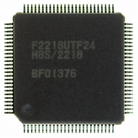
Manufacturer Part Number
HD64F2218UTF24
Description
IC H8S MCU FLASH 128K 100-TQFP
Manufacturer
Renesas Electronics America
Series
H8® H8S/2200r
Specifications of HD64F2218UTF24
Core Processor
H8S/2000
Core Size
16-Bit
Speed
24MHz
Connectivity
SCI, SmartCard, USB
Peripherals
DMA, POR, PWM, WDT
Number Of I /o
69
Program Memory Size
128KB (128K x 8)
Program Memory Type
FLASH
Ram Size
12K x 8
Voltage - Supply (vcc/vdd)
2.7 V ~ 3.6 V
Data Converters
A/D 6x10b
Oscillator Type
Internal
Operating Temperature
-20°C ~ 75°C
Package / Case
100-TQFP, 100-VQFP
For Use With
3DK2218-SS - KIT DEV H8S/2218 WINDOWS SIDESHW
Lead Free Status / RoHS Status
Contains lead / RoHS non-compliant
Eeprom Size
-
Available stocks
Company
Part Number
Manufacturer
Quantity
Price

Part Number:
HD64F2218UTF24V
Manufacturer:
RENESAS/瑞萨
Quantity:
20 000


Section 9 16-Bit Timer Pulse Unit (TPU)
Figure 9.1
Figure 9.2
Figure 9.3
Figure 9.4
Figure 9.5
Figure 9.6
Figure 9.7
Figure 9.8
Figure 9.9
Figure 9.10 Example of 0 Output/1 Output Operation............................................................... 304
Figure 9.11 Example of Toggle Output Operation..................................................................... 304
Figure 9.12 Example of Input Capture Operation Setting Procedure......................................... 305
Figure 9.13 Example of Input Capture Operation...................................................................... 306
Figure 9.14 Example of Synchronous Operation Setting Procedure.......................................... 307
Figure 9.15 Example of Synchronous Operation ....................................................................... 308
Figure 9.16 Compare Match Buffer Operation .......................................................................... 309
Figure 9.17 Input Capture Buffer Operation .............................................................................. 309
Figure 9.18 Example of Buffer Operation Setting Procedure .................................................... 310
Figure 9.19 Example of Buffer Operation (1)............................................................................ 311
Figure 9.20 Example of Buffer Operation (2)............................................................................ 312
Figure 9.21 Example of PWM Mode Setting Procedure............................................................ 314
Figure 9.22 Example of PWM Mode Operation (1) .................................................................. 315
Figure 9.23 Example of PWM Mode Operation (2) .................................................................. 315
Figure 9.24 Example of PWM Mode Operation (3) .................................................................. 316
Figure 9.25 Example of Phase Counting Mode Setting Procedure ............................................ 317
Figure 9.26 Example of Phase Counting Mode 1 Operation...................................................... 318
Figure 9.27 Example of Phase Counting Mode 2 Operation...................................................... 319
Figure 9.28 Example of Phase Counting Mode 3 Operation...................................................... 320
Figure 9.29 Example of Phase Counting Mode 4 Operation...................................................... 321
Figure 9.30 Count Timing in Internal Clock Operation ............................................................. 324
Figure 9.31 Count Timing in External Clock Operation............................................................ 324
Figure 9.32 Output Compare Output Timing............................................................................. 325
Figure 9.33 Input Capture Input Signal Timing ......................................................................... 325
Figure 9.34 Counter Clear Timing (Compare Match)................................................................ 326
Figure 9.35 Counter Clear Timing (Input Capture) ................................................................... 326
Figure 9.36 Buffer Operation Timing (Compare Match)........................................................... 327
Figure 9.37 Buffer Operation Timing (Input Capture)............................................................... 327
Figure 9.38 TGI Interrupt Timing (Compare Match)................................................................. 328
Figure 9.39 TGI Interrupt Timing (Input Capture) .................................................................... 328
Figure 9.40 TCIV Interrupt Setting Timing ............................................................................... 329
Rev.7.00 Dec. 24, 2008 Page xl of liv
REJ09B0074-0700
Block Diagram of TPU ........................................................................................... 274
16-Bit Register Access Operation [Bus Master ↔ TCNT (16 Bits)] ..................... 299
8-Bit Register Access Operation [Bus Master ↔ TCR (Upper 8 Bits)] ................. 300
8-Bit Register Access Operation [Bus Master ↔ TMDR (Lower 8 Bits)]............. 300
8-Bit Register Access Operation [Bus Master ↔ TCR and TMDR (16 Bits)]....... 300
Example of Counter Operation Setting Procedure.................................................. 301
Free-Running Counter Operation ........................................................................... 302
Periodic Counter Operation .................................................................................... 303
Example of Setting Procedure for Waveform Output by Compare Match ............. 303
Related parts for HD64F2218UTF24
Image
Part Number
Description
Manufacturer
Datasheet
Request
R

Part Number:
Description:
KIT STARTER FOR M16C/29
Manufacturer:
Renesas Electronics America
Datasheet:

Part Number:
Description:
KIT STARTER FOR R8C/2D
Manufacturer:
Renesas Electronics America
Datasheet:

Part Number:
Description:
R0K33062P STARTER KIT
Manufacturer:
Renesas Electronics America
Datasheet:

Part Number:
Description:
KIT STARTER FOR R8C/23 E8A
Manufacturer:
Renesas Electronics America
Datasheet:

Part Number:
Description:
KIT STARTER FOR R8C/25
Manufacturer:
Renesas Electronics America
Datasheet:

Part Number:
Description:
KIT STARTER H8S2456 SHARPE DSPLY
Manufacturer:
Renesas Electronics America
Datasheet:

Part Number:
Description:
KIT STARTER FOR R8C38C
Manufacturer:
Renesas Electronics America
Datasheet:

Part Number:
Description:
KIT STARTER FOR R8C35C
Manufacturer:
Renesas Electronics America
Datasheet:

Part Number:
Description:
KIT STARTER FOR R8CL3AC+LCD APPS
Manufacturer:
Renesas Electronics America
Datasheet:
Part Number:
Description:
KIT STARTER FOR RX610
Manufacturer:
Renesas Electronics America
Datasheet:

Part Number:
Description:
KIT STARTER FOR R32C/118
Manufacturer:
Renesas Electronics America
Datasheet:

Part Number:
Description:
KIT DEV RSK-R8C/26-29
Manufacturer:
Renesas Electronics America
Datasheet:

Part Number:
Description:
KIT STARTER FOR SH7124
Manufacturer:
Renesas Electronics America
Datasheet:

Part Number:
Description:
KIT STARTER FOR H8SX/1622
Manufacturer:
Renesas Electronics America
Datasheet:

Part Number:
Description:
KIT DEV FOR SH7203
Manufacturer:
Renesas Electronics America
Datasheet: