HD64F2218UTF24 Renesas Electronics America, HD64F2218UTF24 Datasheet - Page 482
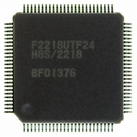
HD64F2218UTF24
Manufacturer Part Number
HD64F2218UTF24
Description
IC H8S MCU FLASH 128K 100-TQFP
Manufacturer
Renesas Electronics America
Series
H8® H8S/2200r
Specifications of HD64F2218UTF24
Core Processor
H8S/2000
Core Size
16-Bit
Speed
24MHz
Connectivity
SCI, SmartCard, USB
Peripherals
DMA, POR, PWM, WDT
Number Of I /o
69
Program Memory Size
128KB (128K x 8)
Program Memory Type
FLASH
Ram Size
12K x 8
Voltage - Supply (vcc/vdd)
2.7 V ~ 3.6 V
Data Converters
A/D 6x10b
Oscillator Type
Internal
Operating Temperature
-20°C ~ 75°C
Package / Case
100-TQFP, 100-VQFP
For Use With
3DK2218-SS - KIT DEV H8S/2218 WINDOWS SIDESHW
Lead Free Status / RoHS Status
Contains lead / RoHS non-compliant
Eeprom Size
-
Available stocks
Company
Part Number
Manufacturer
Quantity
Price

Part Number:
HD64F2218UTF24V
Manufacturer:
RENESAS/瑞萨
Quantity:
20 000


Rev.7.00 Dec. 24, 2008 Page 426 of 698
REJ09B0074-0700
Note: When switching from transmit or receive operation to simultaneous
transmit and receive operations, first clear the TE bit and RE bit to 0,
then set both these bits to 1 simultaneously.
Figure 12.23 Sample Flowchart of Simultaneous Serial Data Transmit and
No
No
No
Clear TE and RE bits in SCR to 0
Read receive data in RDR, and
Write transmit data to TDR and
clear TDRE flag in SSR to 0
clear RDRF flag in SSR to 0
Start transmission/reception
Read ORER flag in SSR
Read TDRE flag in SSR
Read RDRF flag in SSR
All data received?
Initialization
ORER = 1
TDRE = 1
RDRF = 1
<End>
Yes
Yes
Yes
No
Receive Operations
Error processing
Yes
[1]
[2]
[4]
[5]
[3]
[1]
[2]
[3]
[4]
[5]
SCI initialization:
The TxD pin is designated as the
transmit data output pin, and the RxD pin
is designated as the receive data input
pin, enabling simultaneous transmit and
receive operations.
SCI status check and transmit data write:
Read SSR and check that the TDRE flag
is set to 1, then write transmit data to
TDR and clear the TDRE flag to 0.
Transition of the TDRE flag from 0 to 1
can also be identified by a TXI interrupt.
Receive error processing:
If a receive error occurs, read the ORER
flag in SSR, and after performing the
appropriate error processing, clear the
ORER flag to 0. Transmission/reception
cannot be resumed if the ORER flag is
set to 1.
SCI status check and receive data read:
Read SSR and check that the RDRF flag
is set to 1, then read the receive data in
RDR and clear the RDRF flag to 0.
Transition of the RDRF flag from 0 to 1
can also be identified by an RXI
interrupt.
Serial transmission/reception
continuation procedure:
To continue serial transmission/
reception, before the MSB (bit 7) of the
current frame is received, finish reading
the RDRF flag, reading RDR, and
clearing the RDRF flag to 0. Also,
before the MSB (bit 7) of the current
frame is transmitted, read 1 from the
TDRE flag to confirm that writing is
possible. Then write data to TDR and
clear the TDRE flag to 0.
Checking and clearing of the TDRE flag
is automatic when the DMAC is activated
by a transmit data empty interrupt (TXI)
request and data is written to TDR.
Also, the RDRF flag is cleared
automatically when the DMAC is
activated by a receive data full interrupt
(RXI) request and the RDR value is
read.
Related parts for HD64F2218UTF24
Image
Part Number
Description
Manufacturer
Datasheet
Request
R

Part Number:
Description:
KIT STARTER FOR M16C/29
Manufacturer:
Renesas Electronics America
Datasheet:

Part Number:
Description:
KIT STARTER FOR R8C/2D
Manufacturer:
Renesas Electronics America
Datasheet:

Part Number:
Description:
R0K33062P STARTER KIT
Manufacturer:
Renesas Electronics America
Datasheet:

Part Number:
Description:
KIT STARTER FOR R8C/23 E8A
Manufacturer:
Renesas Electronics America
Datasheet:

Part Number:
Description:
KIT STARTER FOR R8C/25
Manufacturer:
Renesas Electronics America
Datasheet:

Part Number:
Description:
KIT STARTER H8S2456 SHARPE DSPLY
Manufacturer:
Renesas Electronics America
Datasheet:

Part Number:
Description:
KIT STARTER FOR R8C38C
Manufacturer:
Renesas Electronics America
Datasheet:

Part Number:
Description:
KIT STARTER FOR R8C35C
Manufacturer:
Renesas Electronics America
Datasheet:

Part Number:
Description:
KIT STARTER FOR R8CL3AC+LCD APPS
Manufacturer:
Renesas Electronics America
Datasheet:
Part Number:
Description:
KIT STARTER FOR RX610
Manufacturer:
Renesas Electronics America
Datasheet:

Part Number:
Description:
KIT STARTER FOR R32C/118
Manufacturer:
Renesas Electronics America
Datasheet:

Part Number:
Description:
KIT DEV RSK-R8C/26-29
Manufacturer:
Renesas Electronics America
Datasheet:

Part Number:
Description:
KIT STARTER FOR SH7124
Manufacturer:
Renesas Electronics America
Datasheet:

Part Number:
Description:
KIT STARTER FOR H8SX/1622
Manufacturer:
Renesas Electronics America
Datasheet:

Part Number:
Description:
KIT DEV FOR SH7203
Manufacturer:
Renesas Electronics America
Datasheet: