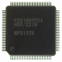
HD64F2218UTF24 Renesas Electronics America, HD64F2218UTF24 Datasheet - Page 651

HD64F2218UTF24
Manufacturer Part Number
HD64F2218UTF24
Description
IC H8S MCU FLASH 128K 100-TQFP
Manufacturer
Renesas Electronics America
Series
H8® H8S/2200r
Specifications of HD64F2218UTF24
Core Processor
H8S/2000
Core Size
16-Bit
Speed
24MHz
Connectivity
SCI, SmartCard, USB
Peripherals
DMA, POR, PWM, WDT
Number Of I /o
69
Program Memory Size
128KB (128K x 8)
Program Memory Type
FLASH
Ram Size
12K x 8
Voltage - Supply (vcc/vdd)
2.7 V ~ 3.6 V
Data Converters
A/D 6x10b
Oscillator Type
Internal
Operating Temperature
-20°C ~ 75°C
Package / Case
100-TQFP, 100-VQFP
For Use With
3DK2218-SS - KIT DEV H8S/2218 WINDOWS SIDESHW
Lead Free Status / RoHS Status
Contains lead / RoHS non-compliant
Eeprom Size
-
Available stocks
Company
Part Number
Manufacturer
Quantity
Price
Part Number:
HD64F2218UTF24V
Manufacturer:
RENESAS/瑞萨
Quantity:
20 000
- Current page: 651 of 758
- Download datasheet (5Mb)
This LSI has an on-chip clock pulse generator that generates the system clock (φ), the bus master
clock, and internal clocks. The clock pulse generator consists of a main clock oscillator, duty
adjustment circuit, clock select circuit, medium-speed clock divider, bus master clock selection
circuit, subclock oscillator, waveform shaping circuit, PLL (Phase Locked Loop) circuit, and USB
operating clock selection circuit. A block diagram of clock pulse generator is shown in figure
19.1.
The frequency of the main clock oscillator can be changed by software by means of settings in the
low-power control register (LPWRCR) and system clock control register (SCKCR). PLL 48-MHz
clock can be selected by software by means of setting the USB control register (UCTLR). For
details, refer to section 14, Universal Serial Bus (USB).
CPG0600B_000020020900
EXTAL
XTAL
OSC1
OSC2
Legend:
LPWRCR: Low power control register
SCKCR:
UCTLR:
UCKS3 to UCKS0
oscillator
Subclock
oscillator
System clock control register
USB control register
clock
Main
selection circuit
operation
UCTLR
circuit
USB
clock
PLL
Figure 19.1 Block Diagram of Clock Pulse Generator
Section 19 Clock Pulse Generator
adjustment
LPWRCR
generation
Waveform
circuit
Duty
circuit
USB operation
48MHz
RFCUT
to USB
clock
RTC clock
to RTC
φ SUB
φ
selection
Clock
circuit
System clock
to φ pin
Rev.7.00 Dec. 24, 2008 Page 595 of 698
clock divider
Medium-
speed
Internal clock
to peripheral
modules
SCK2 to SCK0
φ/2
to φ/32
φ
selection
SCKCR
master
REJ09B0074-0700
circuit
clock
Bus
Bus master clock
USB clock
to USB
to CPU,
DMAC
Related parts for HD64F2218UTF24
Image
Part Number
Description
Manufacturer
Datasheet
Request
R

Part Number:
Description:
KIT STARTER FOR M16C/29
Manufacturer:
Renesas Electronics America
Datasheet:

Part Number:
Description:
KIT STARTER FOR R8C/2D
Manufacturer:
Renesas Electronics America
Datasheet:

Part Number:
Description:
R0K33062P STARTER KIT
Manufacturer:
Renesas Electronics America
Datasheet:

Part Number:
Description:
KIT STARTER FOR R8C/23 E8A
Manufacturer:
Renesas Electronics America
Datasheet:

Part Number:
Description:
KIT STARTER FOR R8C/25
Manufacturer:
Renesas Electronics America
Datasheet:

Part Number:
Description:
KIT STARTER H8S2456 SHARPE DSPLY
Manufacturer:
Renesas Electronics America
Datasheet:

Part Number:
Description:
KIT STARTER FOR R8C38C
Manufacturer:
Renesas Electronics America
Datasheet:

Part Number:
Description:
KIT STARTER FOR R8C35C
Manufacturer:
Renesas Electronics America
Datasheet:

Part Number:
Description:
KIT STARTER FOR R8CL3AC+LCD APPS
Manufacturer:
Renesas Electronics America
Datasheet:

Part Number:
Description:
KIT STARTER FOR RX610
Manufacturer:
Renesas Electronics America
Datasheet:

Part Number:
Description:
KIT STARTER FOR R32C/118
Manufacturer:
Renesas Electronics America
Datasheet:

Part Number:
Description:
KIT DEV RSK-R8C/26-29
Manufacturer:
Renesas Electronics America
Datasheet:

Part Number:
Description:
KIT STARTER FOR SH7124
Manufacturer:
Renesas Electronics America
Datasheet:

Part Number:
Description:
KIT STARTER FOR H8SX/1622
Manufacturer:
Renesas Electronics America
Datasheet:

Part Number:
Description:
KIT DEV FOR SH7203
Manufacturer:
Renesas Electronics America
Datasheet:


