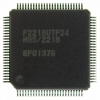
HD64F2218UTF24 Renesas Electronics America, HD64F2218UTF24 Datasheet - Page 441

HD64F2218UTF24
Manufacturer Part Number
HD64F2218UTF24
Description
IC H8S MCU FLASH 128K 100-TQFP
Manufacturer
Renesas Electronics America
Series
H8® H8S/2200r
Specifications of HD64F2218UTF24
Core Processor
H8S/2000
Core Size
16-Bit
Speed
24MHz
Connectivity
SCI, SmartCard, USB
Peripherals
DMA, POR, PWM, WDT
Number Of I /o
69
Program Memory Size
128KB (128K x 8)
Program Memory Type
FLASH
Ram Size
12K x 8
Voltage - Supply (vcc/vdd)
2.7 V ~ 3.6 V
Data Converters
A/D 6x10b
Oscillator Type
Internal
Operating Temperature
-20°C ~ 75°C
Package / Case
100-TQFP, 100-VQFP
For Use With
3DK2218-SS - KIT DEV H8S/2218 WINDOWS SIDESHW
Lead Free Status / RoHS Status
Contains lead / RoHS non-compliant
Eeprom Size
-
Available stocks
Company
Part Number
Manufacturer
Quantity
Price
Part Number:
HD64F2218UTF24V
Manufacturer:
RENESAS/瑞萨
Quantity:
20 000
- Current page: 441 of 758
- Download datasheet (5Mb)
Bit
3
2
1
0
Bit Name Initial Value R/W Description
ABCS
ACS2
ACS1
ACS0
0
0
0
0
R/W Asynchronous Base Clock Select
R/W
R/W
R/W
Selects the 1-bit-interval base clock in asynchronous mode.
The ABCS setting is valid in asynchronous mode (C/A = 0
in SMR).
0: SCI_0 operates on base clock with frequency of 16
1: SCI_0 operates on base clock with frequency of 8 times
Asynchronous Clock Source Select 2 to 0
These bits select the clock source in asynchronous mode
depending on the combination with the bit 7 (ACS3) in
SEMRB_0 (serial extended mode register B_0). When an
average transfer rate is selected, the base clock is set
automatically regardless of the ABCS value. Note that
average transfer rates support only 10.667 MHz, 16 MHz,
and 24 MHz, and not support other operating frequencies.
Set ACS3 to ACS0 when inputting the external clock (the
CKE1 bit in the SCR register is 1) in asynchronous mode
(the C/A bit in the SMR register is 0). Figures 12.3 and 12.4
show the setting examples.
ACS 3210
times transfer rate
transfer rate
0000: External clock input
0001: 115.152 kbps average transfer rate (for φ =
0010: 460.606 kbps average transfer rate (for φ =
0011: 921.569 kbps average transfer rate (for φ = 16
0100: TPU clock input
10.667 MHz only) is selected (SCI_0 operates
on base clock with frequency of 16 times
transfer rate)
10.667 MHz only) is selected (SCI_0 operates
on base clock with frequency of eight times
transfer rate)
MHz only) is selected (SCI_0 operates on base
clock with frequency of eight times transfer rate)
The signal generated by TIOCA0, TIOCC0,
TIOCA1, and TIOCA2, which are the compare
match outputs for TPU_0 to TPU_2 or PWM
outputs, is used as a base clock. Note that
IRQ0 and IRQ1 cannot be used since TIOCA1
and TIOCA2 are used as outputs.
Rev.7.00 Dec. 24, 2008 Page 385 of 698
REJ09B0074-0700
Related parts for HD64F2218UTF24
Image
Part Number
Description
Manufacturer
Datasheet
Request
R

Part Number:
Description:
KIT STARTER FOR M16C/29
Manufacturer:
Renesas Electronics America
Datasheet:

Part Number:
Description:
KIT STARTER FOR R8C/2D
Manufacturer:
Renesas Electronics America
Datasheet:

Part Number:
Description:
R0K33062P STARTER KIT
Manufacturer:
Renesas Electronics America
Datasheet:

Part Number:
Description:
KIT STARTER FOR R8C/23 E8A
Manufacturer:
Renesas Electronics America
Datasheet:

Part Number:
Description:
KIT STARTER FOR R8C/25
Manufacturer:
Renesas Electronics America
Datasheet:

Part Number:
Description:
KIT STARTER H8S2456 SHARPE DSPLY
Manufacturer:
Renesas Electronics America
Datasheet:

Part Number:
Description:
KIT STARTER FOR R8C38C
Manufacturer:
Renesas Electronics America
Datasheet:

Part Number:
Description:
KIT STARTER FOR R8C35C
Manufacturer:
Renesas Electronics America
Datasheet:

Part Number:
Description:
KIT STARTER FOR R8CL3AC+LCD APPS
Manufacturer:
Renesas Electronics America
Datasheet:

Part Number:
Description:
KIT STARTER FOR RX610
Manufacturer:
Renesas Electronics America
Datasheet:

Part Number:
Description:
KIT STARTER FOR R32C/118
Manufacturer:
Renesas Electronics America
Datasheet:

Part Number:
Description:
KIT DEV RSK-R8C/26-29
Manufacturer:
Renesas Electronics America
Datasheet:

Part Number:
Description:
KIT STARTER FOR SH7124
Manufacturer:
Renesas Electronics America
Datasheet:

Part Number:
Description:
KIT STARTER FOR H8SX/1622
Manufacturer:
Renesas Electronics America
Datasheet:

Part Number:
Description:
KIT DEV FOR SH7203
Manufacturer:
Renesas Electronics America
Datasheet:


