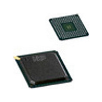
PNX1500E NXP Semiconductors, PNX1500E Datasheet - Page 249

PNX1500E
Manufacturer Part Number
PNX1500E
Description
Manufacturer
NXP Semiconductors
Datasheet
1.PNX1500E.pdf
(828 pages)
Specifications of PNX1500E
Lead Free Status / Rohs Status
Not Compliant
Available stocks
Company
Part Number
Manufacturer
Quantity
Price
Company:
Part Number:
PNX1500E
Manufacturer:
NORTEL
Quantity:
1 000
- Current page: 249 of 828
- Download datasheet (4Mb)
NXP Semiconductors
Volume 1 of 1
Table 8: Registers Description
PNX15XX_PNX952X_SER_N_4
Product data sheet
Bit
2:0
Offset 0x04 0094—07FC Reserved
Offset 0x04 0800
This register will accept only word writes.
31:0
Offset 0x04 0804
This register will accept only word writes.
31:0
Offset 0x04 0808
This register will accept any size writes.
31:16
15:0
Offset 0x04 080C
This register will accept any size writes.
31:11
10
9
8
Symbol
dma_fetch
dma_eaddr
dma_iaddr
Reserved
dma_length
Reserved
single_data_phase
snd2xio
fix_addr
DMA PCI Address
DMA Internal Address
DMA Transfer Size
DMA Controls
Acces
s
R/W
R/W
R/W
R/W
R/W
R
R/W
R/W
R/W
Value
2
1C00_00
00
0010_00
00
0
800
0
0
0
0
Rev. 4.0 — 03 December 2007
Description
Encoded DMA DTL read block size
siz read_block_siz
0:
1:
2:
3:
4: 128 bytes
5: 256 bytes
6: 512 bytes
7: 1024 bytes
Recommended for high bandwidth value 4.
This is the external starting address for the DMA engine. It is used
for DMA transfers over PCI and XIO. Bit 0 and 1 are not used
because all DMA transfers are word aligned.
This is the internal read source/ write destination address in
SDRAM.
This is the length of the DMA transfer (number of 4-byte words).
1 = Limit DMA to single data phase transactions.
0 = Use max_burst_size to determine burst size.
0 = DMA will target PCI.
1 = DMA will target XIO.
0 = DMA will use linear address.
1 = DMA will use a fixed address.
16 bytes
32 bytes
64 bytes
This overrides “max_burst_size.”
8 bytes
PNX15xx/952x Series
Chapter 7: PCI-XIO Module
© NXP B.V. 2007. All rights reserved.
7-249
Related parts for PNX1500E
Image
Part Number
Description
Manufacturer
Datasheet
Request
R
Part Number:
Description:
NXP Semiconductors designed the LPC2420/2460 microcontroller around a 16-bit/32-bitARM7TDMI-S CPU core with real-time debug interfaces that include both JTAG andembedded trace
Manufacturer:
NXP Semiconductors
Datasheet:

Part Number:
Description:
NXP Semiconductors designed the LPC2458 microcontroller around a 16-bit/32-bitARM7TDMI-S CPU core with real-time debug interfaces that include both JTAG andembedded trace
Manufacturer:
NXP Semiconductors
Datasheet:
Part Number:
Description:
NXP Semiconductors designed the LPC2468 microcontroller around a 16-bit/32-bitARM7TDMI-S CPU core with real-time debug interfaces that include both JTAG andembedded trace
Manufacturer:
NXP Semiconductors
Datasheet:
Part Number:
Description:
NXP Semiconductors designed the LPC2470 microcontroller, powered by theARM7TDMI-S core, to be a highly integrated microcontroller for a wide range ofapplications that require advanced communications and high quality graphic displays
Manufacturer:
NXP Semiconductors
Datasheet:
Part Number:
Description:
NXP Semiconductors designed the LPC2478 microcontroller, powered by theARM7TDMI-S core, to be a highly integrated microcontroller for a wide range ofapplications that require advanced communications and high quality graphic displays
Manufacturer:
NXP Semiconductors
Datasheet:
Part Number:
Description:
The Philips Semiconductors XA (eXtended Architecture) family of 16-bit single-chip microcontrollers is powerful enough to easily handle the requirements of high performance embedded applications, yet inexpensive enough to compete in the market for hi
Manufacturer:
NXP Semiconductors
Datasheet:
Part Number:
Description:
The XA-S3 device is a member of Philips Semiconductors? XA(eXtended Architecture) family of high performance 16-bitsingle-chip microcontrollers
Manufacturer:
NXP Semiconductors
Datasheet:

Part Number:
Description:
The NXP BlueStreak LH75401/LH75411 family consists of two low-cost 16/32-bit System-on-Chip (SoC) devices
Manufacturer:
NXP Semiconductors
Datasheet:

Part Number:
Description:
The NXP LPC3130/3131 combine an 180 MHz ARM926EJ-S CPU core, high-speed USB2
Manufacturer:
NXP Semiconductors
Datasheet:

Part Number:
Description:
The NXP LPC3141 combine a 270 MHz ARM926EJ-S CPU core, High-speed USB 2
Manufacturer:
NXP Semiconductors

Part Number:
Description:
The NXP LPC3143 combine a 270 MHz ARM926EJ-S CPU core, High-speed USB 2
Manufacturer:
NXP Semiconductors

Part Number:
Description:
The NXP LPC3152 combines an 180 MHz ARM926EJ-S CPU core, High-speed USB 2
Manufacturer:
NXP Semiconductors

Part Number:
Description:
The NXP LPC3154 combines an 180 MHz ARM926EJ-S CPU core, High-speed USB 2
Manufacturer:
NXP Semiconductors

Part Number:
Description:
Standard level N-channel enhancement mode Field-Effect Transistor (FET) in a plastic package using NXP High-Performance Automotive (HPA) TrenchMOS technology
Manufacturer:
NXP Semiconductors
Datasheet:


