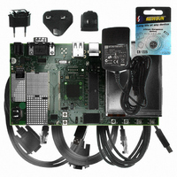
AT91SAM9G10-EK Atmel, AT91SAM9G10-EK Datasheet - Page 715

AT91SAM9G10-EK
Manufacturer Part Number
AT91SAM9G10-EK
Description
KIT DEV FOR SAM9G10 ARM
Manufacturer
Atmel
Type
MCUr
Specifications of AT91SAM9G10-EK
Contents
Board, Cables, Power Supply
Silicon Manufacturer
Atmel
Core Architecture
AVR
Kit Contents
Board
Svhc
No SVHC (15-Dec-2010)
Mcu Supported Families
AT91SAM9G10, ARM926EJ-S
Tool / Board Applications
Microcontroller
Rohs Compliant
Yes
For Use With/related Products
*
Lead Free Status / RoHS Status
Contains lead / RoHS non-compliant
- Current page: 715 of 730
- Download datasheet (12Mb)
42.2.7.4
42.2.8
42.2.8.1
42.2.9
42.2.9.1
42.2.10
42.2.10.1
6462A–ATARM–03-Jun-09
Shutdown Controller (SHDWC)
Static Memory Controller (SMC)
System Controller
SHDWC: Boundary Scan Mode Outputs the 32 kHz clock
SMC: Chip Select Parameters Modification
SYSC: Possible Event Loss when Reading RTT_SR
SSC: First RK Clock Cycle when Rk Outputs a Clock During Data Transfer
At the end of the data, the RK pin is set in high impedance which might be seen as an unex-
pected clock cycle.
Enable the pull-up on RK pin.
When the SSC receiver is used with the following conditions:
The first clock cycle time generated by the RK pin is equal to MCK/(2 x (value +1)).
None.
In boundary scan mode, the SHDN pin outputs the 32 kHz clock.
There is only one way to disable the 32 kHz clock on the SHDN pin.
In boundary scan mode, connect TST and JTAGSEL pins to VDDBU and set the SHDN pin to
low level.
The user must not change the configuration parameters of an SMC Chip Select (Setup, Pulse,
Cycle, Mode) if accesses are performed on this CS during the modification.
For example, the modification of the Chip Select 0 (CS0) parameters, while fetching the code
from a memory connected on this CS0, may lead to unpredictable behavior.
The code used to modify the parameters of an SMC Chip Select can be executed from the inter-
nal RAM or from a memory connected to another Chip Select
If an event (RTTINC or ALMS) occurs within the same slow clock cycle as when the RTT_SR is
read, the corresponding bit might be cleared. This can lead to the loss of this event.
The software must handle an RTT event as interrupt and as the only source of the interrupt
source level 1.
• data sampled on RK falling edge (CKI = 0),
• RX clock is divided clock (CKS = 0 and DIV different from 0)
• RK pin set as output and provides the clock during data transfer (CKO = 2)
• data sampled on RK falling edge (CKI = 0),
Problem Fix/Workaround
Problem Fix/Workaround
Problem/Fix Workaround
Problem Fix/Workaround
Problem Fix/Workaround
AT91SAM9G10
715
Related parts for AT91SAM9G10-EK
Image
Part Number
Description
Manufacturer
Datasheet
Request
R

Part Number:
Description:
MCU, MPU & DSP Development Tools KICKSTART KIT FOR AT91SAM9 PLUS
Manufacturer:
IAR Systems

Part Number:
Description:
DEV KIT FOR AVR/AVR32
Manufacturer:
Atmel
Datasheet:

Part Number:
Description:
INTERVAL AND WIPE/WASH WIPER CONTROL IC WITH DELAY
Manufacturer:
ATMEL Corporation
Datasheet:

Part Number:
Description:
Low-Voltage Voice-Switched IC for Hands-Free Operation
Manufacturer:
ATMEL Corporation
Datasheet:

Part Number:
Description:
MONOLITHIC INTEGRATED FEATUREPHONE CIRCUIT
Manufacturer:
ATMEL Corporation
Datasheet:

Part Number:
Description:
AM-FM Receiver IC U4255BM-M
Manufacturer:
ATMEL Corporation
Datasheet:

Part Number:
Description:
Monolithic Integrated Feature Phone Circuit
Manufacturer:
ATMEL Corporation
Datasheet:

Part Number:
Description:
Multistandard Video-IF and Quasi Parallel Sound Processing
Manufacturer:
ATMEL Corporation
Datasheet:

Part Number:
Description:
High-performance EE PLD
Manufacturer:
ATMEL Corporation
Datasheet:

Part Number:
Description:
8-bit Flash Microcontroller
Manufacturer:
ATMEL Corporation
Datasheet:

Part Number:
Description:
2-Wire Serial EEPROM
Manufacturer:
ATMEL Corporation
Datasheet:


