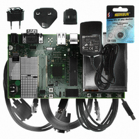
AT91SAM9G10-EK Atmel, AT91SAM9G10-EK Datasheet - Page 357

AT91SAM9G10-EK
Manufacturer Part Number
AT91SAM9G10-EK
Description
KIT DEV FOR SAM9G10 ARM
Manufacturer
Atmel
Type
MCUr
Specifications of AT91SAM9G10-EK
Contents
Board, Cables, Power Supply
Silicon Manufacturer
Atmel
Core Architecture
AVR
Kit Contents
Board
Svhc
No SVHC (15-Dec-2010)
Mcu Supported Families
AT91SAM9G10, ARM926EJ-S
Tool / Board Applications
Microcontroller
Rohs Compliant
Yes
For Use With/related Products
*
Lead Free Status / RoHS Status
Contains lead / RoHS non-compliant
- Current page: 357 of 730
- Download datasheet (12Mb)
30.6.3.7
30.6.3.8
6462A–ATARM–03-Jun-09
Transfer Size
Peripheral Chip Select Decoding
ever the SPI still controls the number of bits (8 to16) to be transferred through MISO and MOSI
lines with the chip select configuration registers. This is not the optimal means in term of mem-
ory size for the buffers, but it provides a very effective means to exchange data with several
peripherals without any intervention of the processor.
Depending on the data size to transmit, from 8 to 16 bits, the PDC manages automatically the
type of pointer's size it has to point to. The PDC will perform the following transfer size depend-
ing on the mode and number of bits per data.
Fixed Mode:
Variable Mode:
In variable Mode, PDC Pointer Address = Address +4 bytes and PDC Counter = Counter - 1 for
8 to 16-bit transfer size. When using the PDC, the TDRE and RDRF flags are handled by the
PDC, thus the user’s application does not have to check those bits. Only End of RX Buffer
(ENDRX), End of TX Buffer (ENDTX), Buffer Full (RXBUFF), TX Buffer Empty (TXBUFE) are
significant. For further details about the Peripheral DMA Controller and user interface, refer to
the PDC section of the product datasheet.
The user can program the SPI to operate with up to 15 peripherals by decoding the four Chip
Select lines, NPCS0 to NPCS3 with 1 of up to 16 decoder/demultiplexer. This can be enabled by
writing the PCSDEC bit at 1 in the Mode Register (SPI_MR).
When operating without decoding, the SPI makes sure that in any case only one chip select line
is activated, i.e., one NPCS line driven low at a time. If two bits are defined low in a PCS field,
only the lowest numbered chip select is driven low.
When operating with decoding, the SPI directly outputs the value defined by the PCS field on
NPCS lines of either the Mode Register or the Transmit Data Register (depending on PS).
As the SPI sets a default value of 0xF on the chip select lines (i.e. all chip select lines at 1) when
not processing any transfer, only 15 peripherals can be decoded.
The SPI has only four Chip Select Registers, not 15. As a result, when decoding is activated,
each chip select defines the characteristics of up to four peripherals. As an example, SPI_CRS0
defines the characteristics of the externally decoded peripherals 0 to 3, corresponding to the
PCS values 0x0 to 0x3. Thus, the user has to make sure to connect compatible peripherals on
the decoded chip select lines 0 to 3, 4 to 7, 8 to 11 and 12 to 14.
an implementation.
• 8-bit Data:
• 8-bit to 16-bit Data:
Byte transfer,
PDC Pointer Address = Address + 1 byte,
PDC Counter = Counter - 1
2 bytes transfer. n-bit data transfer with don’t care data (MSB) filled with 0’s,
PDC Pointer Address = Address + 2 bytes,
PDC Counter = Counter - 1
Figure 30-10
AT91SAM9G10
below shows such
357
Related parts for AT91SAM9G10-EK
Image
Part Number
Description
Manufacturer
Datasheet
Request
R

Part Number:
Description:
MCU, MPU & DSP Development Tools KICKSTART KIT FOR AT91SAM9 PLUS
Manufacturer:
IAR Systems

Part Number:
Description:
DEV KIT FOR AVR/AVR32
Manufacturer:
Atmel
Datasheet:

Part Number:
Description:
INTERVAL AND WIPE/WASH WIPER CONTROL IC WITH DELAY
Manufacturer:
ATMEL Corporation
Datasheet:

Part Number:
Description:
Low-Voltage Voice-Switched IC for Hands-Free Operation
Manufacturer:
ATMEL Corporation
Datasheet:

Part Number:
Description:
MONOLITHIC INTEGRATED FEATUREPHONE CIRCUIT
Manufacturer:
ATMEL Corporation
Datasheet:

Part Number:
Description:
AM-FM Receiver IC U4255BM-M
Manufacturer:
ATMEL Corporation
Datasheet:

Part Number:
Description:
Monolithic Integrated Feature Phone Circuit
Manufacturer:
ATMEL Corporation
Datasheet:

Part Number:
Description:
Multistandard Video-IF and Quasi Parallel Sound Processing
Manufacturer:
ATMEL Corporation
Datasheet:

Part Number:
Description:
High-performance EE PLD
Manufacturer:
ATMEL Corporation
Datasheet:

Part Number:
Description:
8-bit Flash Microcontroller
Manufacturer:
ATMEL Corporation
Datasheet:

Part Number:
Description:
2-Wire Serial EEPROM
Manufacturer:
ATMEL Corporation
Datasheet:


