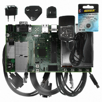
AT91SAM9G10-EK Atmel, AT91SAM9G10-EK Datasheet - Page 640

AT91SAM9G10-EK
Manufacturer Part Number
AT91SAM9G10-EK
Description
KIT DEV FOR SAM9G10 ARM
Manufacturer
Atmel
Type
MCUr
Specifications of AT91SAM9G10-EK
Contents
Board, Cables, Power Supply
Silicon Manufacturer
Atmel
Core Architecture
AVR
Kit Contents
Board
Svhc
No SVHC (15-Dec-2010)
Mcu Supported Families
AT91SAM9G10, ARM926EJ-S
Tool / Board Applications
Microcontroller
Rohs Compliant
Yes
For Use With/related Products
*
Lead Free Status / RoHS Status
Contains lead / RoHS non-compliant
- Current page: 640 of 730
- Download datasheet (12Mb)
Table 38-12. Dithering Algorithm for Color Mode (Continued)
Note:
38.5.2.7
38.5.2.8
640
Frame
N+1
N+1
N+1
N+1
N+1
N+1
N+2
N+2
N+2
N+2
N+2
N+2
…
…
…
Ri = red pixel component ON. Gi = green pixel component ON. Bi = blue pixel component ON. ri = red pixel component OFF.
gi = green pixel component OFF. bi = blue pixel component OFF.
AT91SAM9G10
green_data_0
green_data_1
green_data_0
green_data_1
blue_data_0
blue_data_1
blue_data_0
blue_data_1
Shifter
Timegen
red_data_0
red_data_1
red_data_0
red_data_1
Signal
…
…
…
The FIFO, Serializer, Palette and Dithering modules process one pixel at a time in monochrome
mode and three sub-pixels at a time in color mode (R,G,B components). This module packs the
data according to the output interface. This interface can be programmed in the DISTYPE,
SCANMOD, and IFWIDTH fields of the LCDCON2 register.
The DISTYPE field selects between TFT, STN monochrome and STN color display. The SCAN-
MODE field selects between single and dual scan modes; in TFT mode, only single scan is
supported. The IFWIDTH field configures the width of the interface in STN mode: 4-bit (in single
scan mode only), 8-bit and 16-bit (in dual scan mode only).
For a more detailed description of the fields, see
page
For a more detailed description of the LCD Interface, see
The time generator block generates the control signals LCDDOTCK, LCDHSYNC, LCDVSYNC,
LCDDEN, used by the LCD module. This block is programmable in order to support different
types of LCD modules and obtain the output clock signals, which are derived from the LCDC
Core clock.
The LCDDOTCK signal is used to clock the data into the LCD drivers' shift register. The data is
sent through LCDD[23:0] synchronized by default with LCDDOTCK falling edge (rising edge can
be selected). The CLKVAL field of LCDCON1 register controls the rate of this signal. The divisor
Shadow Level
656.
1010
1010
1010
1010
1010
1010
1010
1010
1010
1010
1010
1010
…
…
…
Bit used
…
…
…
3
2
1
0
3
2
3
2
1
0
3
2
Dithering Pattern
1011
1011
0110
0110
1011
1011
1011
1011
0110
0110
0110
0110
…
…
…
“LCD Controller (LCDC) User Interface” on
4-bit LCDD
“LCD Interface” on page
LCDD[3]
LCDD[2]
LCDD[1]
LCDD[0]
LCDD[3]
LCDD[2]
LCDD[3]
LCDD[2]
LCDD[1]
LCDD[0]
LCDD[3]
LCDD[2]
…
…
…
8-bit LCDD
LCDD[7]
LCDD[6]
LCDD[4]
LCDD[3]
LCDD[7]
LCDD[6]
LCDD[4]
LCDD[3]
LCDD[5]
LCDD[2]
LCDD[5]
LCDD[2]
…
…
…
6462A–ATARM–03-Jun-09
645.
Output
R0
B0
R1
G1
G0
B0
B1
g0
b1
g1
…
…
…
r0
r1
Related parts for AT91SAM9G10-EK
Image
Part Number
Description
Manufacturer
Datasheet
Request
R

Part Number:
Description:
MCU, MPU & DSP Development Tools KICKSTART KIT FOR AT91SAM9 PLUS
Manufacturer:
IAR Systems

Part Number:
Description:
DEV KIT FOR AVR/AVR32
Manufacturer:
Atmel
Datasheet:

Part Number:
Description:
INTERVAL AND WIPE/WASH WIPER CONTROL IC WITH DELAY
Manufacturer:
ATMEL Corporation
Datasheet:

Part Number:
Description:
Low-Voltage Voice-Switched IC for Hands-Free Operation
Manufacturer:
ATMEL Corporation
Datasheet:

Part Number:
Description:
MONOLITHIC INTEGRATED FEATUREPHONE CIRCUIT
Manufacturer:
ATMEL Corporation
Datasheet:

Part Number:
Description:
AM-FM Receiver IC U4255BM-M
Manufacturer:
ATMEL Corporation
Datasheet:

Part Number:
Description:
Monolithic Integrated Feature Phone Circuit
Manufacturer:
ATMEL Corporation
Datasheet:

Part Number:
Description:
Multistandard Video-IF and Quasi Parallel Sound Processing
Manufacturer:
ATMEL Corporation
Datasheet:

Part Number:
Description:
High-performance EE PLD
Manufacturer:
ATMEL Corporation
Datasheet:

Part Number:
Description:
8-bit Flash Microcontroller
Manufacturer:
ATMEL Corporation
Datasheet:

Part Number:
Description:
2-Wire Serial EEPROM
Manufacturer:
ATMEL Corporation
Datasheet:


