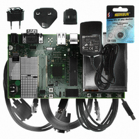
AT91SAM9G10-EK Atmel, AT91SAM9G10-EK Datasheet - Page 642

AT91SAM9G10-EK
Manufacturer Part Number
AT91SAM9G10-EK
Description
KIT DEV FOR SAM9G10 ARM
Manufacturer
Atmel
Type
MCUr
Specifications of AT91SAM9G10-EK
Contents
Board, Cables, Power Supply
Silicon Manufacturer
Atmel
Core Architecture
AVR
Kit Contents
Board
Svhc
No SVHC (15-Dec-2010)
Mcu Supported Families
AT91SAM9G10, ARM926EJ-S
Tool / Board Applications
Microcontroller
Rohs Compliant
Yes
For Use With/related Products
*
Lead Free Status / RoHS Status
Contains lead / RoHS non-compliant
- Current page: 642 of 730
- Download datasheet (12Mb)
38.5.2.9
642
AT91SAM9G10
Equation 1
There is a limitation in the minimum values of VHDLY, HPW and HBP parameters imposed by
the initial latency of the datapath. The total delay in LCDC clock cycles must be higher than or
equal to the latency column in
formula:
where:
The LCDVSYNC is asserted once per frame. This signal is asserted to cause the LCD's line
pointer to start over at the top of the display. The timing of this signal depends on the type of
LCD: STN or TFT LCD.
In STN mode, the high phase corresponds to the complete first line of the frame. In STN mode,
this signal is synchronized with the first active LCDDOTCK rising edge in a line.
In TFT mode, the high phase of this signal starts at the beginning of the first line. The following
timing parameters can be selected:
There are two other parameters to configure in this module, the HOZVAL and the LINEVAL
fields of the LCDFRMCFG:
Figure
SYNC and LCDVSYNC signals:
• VHDLY, HPW, HBP are the value of the fields of LCDTIM1 and LCDTIM2 registers
• PCLK_PERIOD is the period of LCDDOTCK signal measured in LCDC Clock cycles
• DPATH_LATENCY is the datapath latency of the configuration, given in
• Vertical Pulse Width (VPW): LCDVSYNC pulse width is configurable in VPW field of the
• Vertical Back Porch: Number of inactive lines at the beginning of the frame is configurable in
• Vertical Front Porch: Number of inactive lines at the end of the frame is configurable in VFP
• HOZVAL configures the number of active LCDDOTCK cycles in each line. The number of
• LINEVAL configures the number of active lines per frame. This number is equal to
635
LCDTIM1 register. The pulse width is equal to (VPW+1) lines.
VBP field of LCDTIM1 register. The number of inactive lines is equal to VBP. This field should
be programmed with 0 in STN Mode.
field of LCDTIM2 register. The number of inactive lines is equal to VFP. This field should be
programmed with 0 in STN mode.
active cycles in each line is equal to (HOZVAL+1) cycles. The minimum value of this
parameter is 1.
(LINEVAL+1) lines. The minimum value of this parameter is 1.
38-3,
Figure 38-4
(
VHDLY
+
HPW
and
Figure 38-5
+
Table 38-4 on page
HBP
+
3
)
×
show the timing of LCDDOTCK, LCDDEN, LCDH-
PCLK_PERIOD
635. This limitation is given by the following
≥
DPATH_LATENCY
Table 38-4 on page
6462A–ATARM–03-Jun-09
Related parts for AT91SAM9G10-EK
Image
Part Number
Description
Manufacturer
Datasheet
Request
R

Part Number:
Description:
MCU, MPU & DSP Development Tools KICKSTART KIT FOR AT91SAM9 PLUS
Manufacturer:
IAR Systems

Part Number:
Description:
DEV KIT FOR AVR/AVR32
Manufacturer:
Atmel
Datasheet:

Part Number:
Description:
INTERVAL AND WIPE/WASH WIPER CONTROL IC WITH DELAY
Manufacturer:
ATMEL Corporation
Datasheet:

Part Number:
Description:
Low-Voltage Voice-Switched IC for Hands-Free Operation
Manufacturer:
ATMEL Corporation
Datasheet:

Part Number:
Description:
MONOLITHIC INTEGRATED FEATUREPHONE CIRCUIT
Manufacturer:
ATMEL Corporation
Datasheet:

Part Number:
Description:
AM-FM Receiver IC U4255BM-M
Manufacturer:
ATMEL Corporation
Datasheet:

Part Number:
Description:
Monolithic Integrated Feature Phone Circuit
Manufacturer:
ATMEL Corporation
Datasheet:

Part Number:
Description:
Multistandard Video-IF and Quasi Parallel Sound Processing
Manufacturer:
ATMEL Corporation
Datasheet:

Part Number:
Description:
High-performance EE PLD
Manufacturer:
ATMEL Corporation
Datasheet:

Part Number:
Description:
8-bit Flash Microcontroller
Manufacturer:
ATMEL Corporation
Datasheet:

Part Number:
Description:
2-Wire Serial EEPROM
Manufacturer:
ATMEL Corporation
Datasheet:


