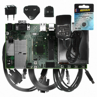
AT91SAM9G10-EK Atmel, AT91SAM9G10-EK Datasheet - Page 240

AT91SAM9G10-EK
Manufacturer Part Number
AT91SAM9G10-EK
Description
KIT DEV FOR SAM9G10 ARM
Manufacturer
Atmel
Type
MCUr
Specifications of AT91SAM9G10-EK
Contents
Board, Cables, Power Supply
Silicon Manufacturer
Atmel
Core Architecture
AVR
Kit Contents
Board
Svhc
No SVHC (15-Dec-2010)
Mcu Supported Families
AT91SAM9G10, ARM926EJ-S
Tool / Board Applications
Microcontroller
Rohs Compliant
Yes
For Use With/related Products
*
Lead Free Status / RoHS Status
Contains lead / RoHS non-compliant
- Current page: 240 of 730
- Download datasheet (12Mb)
Figure 25-4. Divider and PLL Block Diagram
25.4.1
Figure 25-5. PLL Capacitors and Resistors
25.4.2
6462A–ATARM–03-Jun-09
PLL Filter
Divider and Phase Lock Loop Programming
MAINCK
The PLL requires connection to an external second-order filter through the PLLRCA and/or PLL-
RCB pin.
Values of R, C1 and C2 to be connected to the PLLRC pin must be calculated as a function of
the PLL input frequency, the PLL output frequency and the phase margin. A trade-off has to be
found between output signal overshoot and startup time.
The divider can be set between 1 and 255 in steps of 1. When a divider field (DIV) is set to 0, the
output of the corresponding divider and the PLL output is a continuous signal at level 0. On
reset, each DIV field is set to 0, thus the corresponding PLL input clock is set to 0.
SLCK
Figure 25-5
C2
shows a schematic of these filters.
C1
R
Divider B
Divider A
DIVB
DIVA
PLLRC
GND
PLLRCB
PLLRCA
MULB
MULA
PLLBCOUNT
PLLACOUNT
PLL
Counter
Counter
PLL B
PLL A
PLL B
PLL A
OUTB
OUTA
LOCKA
LOCKB
AT91SAM9G10
PLLBCK
PLLACK
240
Related parts for AT91SAM9G10-EK
Image
Part Number
Description
Manufacturer
Datasheet
Request
R

Part Number:
Description:
MCU, MPU & DSP Development Tools KICKSTART KIT FOR AT91SAM9 PLUS
Manufacturer:
IAR Systems

Part Number:
Description:
DEV KIT FOR AVR/AVR32
Manufacturer:
Atmel
Datasheet:

Part Number:
Description:
INTERVAL AND WIPE/WASH WIPER CONTROL IC WITH DELAY
Manufacturer:
ATMEL Corporation
Datasheet:

Part Number:
Description:
Low-Voltage Voice-Switched IC for Hands-Free Operation
Manufacturer:
ATMEL Corporation
Datasheet:

Part Number:
Description:
MONOLITHIC INTEGRATED FEATUREPHONE CIRCUIT
Manufacturer:
ATMEL Corporation
Datasheet:

Part Number:
Description:
AM-FM Receiver IC U4255BM-M
Manufacturer:
ATMEL Corporation
Datasheet:

Part Number:
Description:
Monolithic Integrated Feature Phone Circuit
Manufacturer:
ATMEL Corporation
Datasheet:

Part Number:
Description:
Multistandard Video-IF and Quasi Parallel Sound Processing
Manufacturer:
ATMEL Corporation
Datasheet:

Part Number:
Description:
High-performance EE PLD
Manufacturer:
ATMEL Corporation
Datasheet:

Part Number:
Description:
8-bit Flash Microcontroller
Manufacturer:
ATMEL Corporation
Datasheet:

Part Number:
Description:
2-Wire Serial EEPROM
Manufacturer:
ATMEL Corporation
Datasheet:


