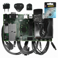
AT91SAM9G10-EK Atmel, AT91SAM9G10-EK Datasheet - Page 639

AT91SAM9G10-EK
Manufacturer Part Number
AT91SAM9G10-EK
Description
KIT DEV FOR SAM9G10 ARM
Manufacturer
Atmel
Type
MCUr
Specifications of AT91SAM9G10-EK
Contents
Board, Cables, Power Supply
Silicon Manufacturer
Atmel
Core Architecture
AVR
Kit Contents
Board
Svhc
No SVHC (15-Dec-2010)
Mcu Supported Families
AT91SAM9G10, ARM926EJ-S
Tool / Board Applications
Microcontroller
Rohs Compliant
Yes
For Use With/related Products
*
Lead Free Status / RoHS Status
Contains lead / RoHS non-compliant
- Current page: 639 of 730
- Download datasheet (12Mb)
Table 38-12. Dithering Algorithm for Color Mode
6462A–ATARM–03-Jun-09
Frame
N
N
N
N
N
N
green_data_0
green_data_1
blue_data_0
blue_data_1
red_data_0
red_data_1
Signal
The same DP_i register can be used for the pairs for which the sum of duty cycles is 1 (e.g., 1/7
and 6/7). The dithering pattern for the first pair member is the inversion of the one for the
second.
The DP_i registers contain a series of 4-bit patterns. The (3-m)
pixel with horizontal coordinate x = 4n + m (n is an integer and m ranges from 0 to 3) should be
turned on or off in the current frame. The operation is shown by the examples below.
Consider the pixels a, b, c and d with the horizontal coordinates 4*n+0, 4*n+1, 4*n+2 and 4*n+3,
respectively. The four pixels should be displayed in gray level 9 (duty cycle 3/5) so the register
used is DP3_5 =”1010 0101 1010 0101 1111”.
The output sequence obtained in the data output for monochrome mode is shown in
11.
Table 38-11. Dithering Algorithm for Monochrome Mode
Consider now color display mode and two pixels p0 and p1 with the horizontal coordinates
4*n+0, and 4*n+1. A color pixel is composed of three components: {R, G, B}. Pixel p0 will be dis-
played sending the color components {R0, G0, B0} to the display. Pixel p1 will be displayed
sending the color components {R1, G1, B1}. Suppose that the data read from memory and
mapped to the lookup tables corresponds to shade level 10 for the three color components of
both pixels, with the dithering pattern to apply to all of them being DP2_3 = “1101 1011 0110”.
Table 38-12
Dual Scan Configuration, each panel data bus acts like in the equivalent single scan
configuration.)
Frame
Number
N
N+1
N+2
N+3
N+4
N+5
N+6
N+7
...
Shadow Level
1010
1010
1010
1010
1010
1010
shows the output sequence in the data output bus for single scan configurations. (In
Pattern
1010
0101
1010
0101
1111
1010
0101
1010
...
Bit used
3
2
1
0
3
2
Pixel a
ON
OFF
ON
OFF
ON
ON
OFF
ON
...
Dithering Pattern
1101
1101
1101
1101
1101
1101
Pixel b
OFF
ON
OFF
ON
ON
OFF
ON
OFF
...
4-bit LCDD
LCDD[3]
LCDD[2]
LCDD[1]
LCDD[0]
LCDD[3]
LCDD[2]
th
bit of the pattern determines if a
Pixel c
ON
OFF
ON
OFF
ON
ON
OFF
ON
...
AT91SAM9G10
8-bit LCDD
LCDD[7]
LCDD[6]
LCDD[5]
LCDD[4]
LCDD[3]
LCDD[2]
OFF
ON
OFF
ON
ON
OFF
ON
OFF
...
Pixel d
Table 38-
Output
G0
G1
R0
R1
B1
b0
639
Related parts for AT91SAM9G10-EK
Image
Part Number
Description
Manufacturer
Datasheet
Request
R

Part Number:
Description:
MCU, MPU & DSP Development Tools KICKSTART KIT FOR AT91SAM9 PLUS
Manufacturer:
IAR Systems

Part Number:
Description:
DEV KIT FOR AVR/AVR32
Manufacturer:
Atmel
Datasheet:

Part Number:
Description:
INTERVAL AND WIPE/WASH WIPER CONTROL IC WITH DELAY
Manufacturer:
ATMEL Corporation
Datasheet:

Part Number:
Description:
Low-Voltage Voice-Switched IC for Hands-Free Operation
Manufacturer:
ATMEL Corporation
Datasheet:

Part Number:
Description:
MONOLITHIC INTEGRATED FEATUREPHONE CIRCUIT
Manufacturer:
ATMEL Corporation
Datasheet:

Part Number:
Description:
AM-FM Receiver IC U4255BM-M
Manufacturer:
ATMEL Corporation
Datasheet:

Part Number:
Description:
Monolithic Integrated Feature Phone Circuit
Manufacturer:
ATMEL Corporation
Datasheet:

Part Number:
Description:
Multistandard Video-IF and Quasi Parallel Sound Processing
Manufacturer:
ATMEL Corporation
Datasheet:

Part Number:
Description:
High-performance EE PLD
Manufacturer:
ATMEL Corporation
Datasheet:

Part Number:
Description:
8-bit Flash Microcontroller
Manufacturer:
ATMEL Corporation
Datasheet:

Part Number:
Description:
2-Wire Serial EEPROM
Manufacturer:
ATMEL Corporation
Datasheet:


