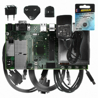
AT91SAM9G10-EK Atmel, AT91SAM9G10-EK Datasheet - Page 635

AT91SAM9G10-EK
Manufacturer Part Number
AT91SAM9G10-EK
Description
KIT DEV FOR SAM9G10 ARM
Manufacturer
Atmel
Type
MCUr
Specifications of AT91SAM9G10-EK
Contents
Board, Cables, Power Supply
Silicon Manufacturer
Atmel
Core Architecture
AVR
Kit Contents
Board
Svhc
No SVHC (15-Dec-2010)
Mcu Supported Families
AT91SAM9G10, ARM926EJ-S
Tool / Board Applications
Microcontroller
Rohs Compliant
Yes
For Use With/related Products
*
Lead Free Status / RoHS Status
Contains lead / RoHS non-compliant
- Current page: 635 of 730
- Download datasheet (12Mb)
38.5.2.3
6462A–ATARM–03-Jun-09
FIFO
The datapath can be characterized by two parameters: initial_latency and cycles_per_data. The
parameter initial_latency is defined as the number of LCDC Core Clock cycles until the first data
is available at the output of the datapath. The parameter cycles_per_data is the minimum num-
ber of LCDC Core clock cycles between two consecutive data at the output interface.
These parameters are different for the different configurations of the LCD Controller and are
shown in
Table 38-4.
The FIFO block buffers the input data read by the DMA module. It contains two input FIFOs to
be used in Dual Scan configuration that are configured as a single FIFO when used in single
scan configuration.
The size of the FIFOs allows a wide range of architectures to be supported.
The upper threshold of the FIFOs can be configured in the FIFOTH field of the LCDFIFO regis-
ter. The LCDC core will request a DMA transfer when the number of words in each FIFO is less
than FIFOTH words. To avoid overwriting in the FIFO and to maximize the FIFO utilization, the
FIFOTH should be programmed with:
where:
TFT
STN Mono
STN Mono
STN Mono
STN Mono
STN Color
STN Color
STN Color
STN Color
• The output interface is a 24-bit data bus. The configuration of this interface depends on the
• The configuration interface connects the datapath with the configuration block. It is used to
• The control interface connects the datapath with the timing generation block. The main
• 512 is the effective size of the FIFO. It is the total FIFO memory size in single scan mode and
• DMA_burst_length is the burst length of the transfers made by the DMA
type of LCD used (TFT or STN, Single or Dual Scan, 4-bit, 8-bit, 16-bit or 24-bit interface).
select between the different datapath configurations.
control signal is the data-request signal, used by the timing generation module to request
new data from the datapath.
half that size in dual scan mode.
DISTYPE
FIFOTH = 512 - (2 x DMA_BURST_LENGTH + 3)
Table
Datapath Parameters
38-4.
SCAN
Single
Single
Dual
Dual
Single
Single
Dual
Dual
Configuration
IFWIDTH
4
8
8
16
4
8
8
16
initial_latency
9
13
17
17
25
11
12
14
15
AT91SAM9G10
cycles_per_data
1
4
8
8
16
2
3
4
6
635
Related parts for AT91SAM9G10-EK
Image
Part Number
Description
Manufacturer
Datasheet
Request
R

Part Number:
Description:
MCU, MPU & DSP Development Tools KICKSTART KIT FOR AT91SAM9 PLUS
Manufacturer:
IAR Systems

Part Number:
Description:
DEV KIT FOR AVR/AVR32
Manufacturer:
Atmel
Datasheet:

Part Number:
Description:
INTERVAL AND WIPE/WASH WIPER CONTROL IC WITH DELAY
Manufacturer:
ATMEL Corporation
Datasheet:

Part Number:
Description:
Low-Voltage Voice-Switched IC for Hands-Free Operation
Manufacturer:
ATMEL Corporation
Datasheet:

Part Number:
Description:
MONOLITHIC INTEGRATED FEATUREPHONE CIRCUIT
Manufacturer:
ATMEL Corporation
Datasheet:

Part Number:
Description:
AM-FM Receiver IC U4255BM-M
Manufacturer:
ATMEL Corporation
Datasheet:

Part Number:
Description:
Monolithic Integrated Feature Phone Circuit
Manufacturer:
ATMEL Corporation
Datasheet:

Part Number:
Description:
Multistandard Video-IF and Quasi Parallel Sound Processing
Manufacturer:
ATMEL Corporation
Datasheet:

Part Number:
Description:
High-performance EE PLD
Manufacturer:
ATMEL Corporation
Datasheet:

Part Number:
Description:
8-bit Flash Microcontroller
Manufacturer:
ATMEL Corporation
Datasheet:

Part Number:
Description:
2-Wire Serial EEPROM
Manufacturer:
ATMEL Corporation
Datasheet:


