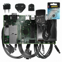
AT91SAM9G10-EK Atmel, AT91SAM9G10-EK Datasheet - Page 633

AT91SAM9G10-EK
Manufacturer Part Number
AT91SAM9G10-EK
Description
KIT DEV FOR SAM9G10 ARM
Manufacturer
Atmel
Type
MCUr
Specifications of AT91SAM9G10-EK
Contents
Board, Cables, Power Supply
Silicon Manufacturer
Atmel
Core Architecture
AVR
Kit Contents
Board
Svhc
No SVHC (15-Dec-2010)
Mcu Supported Families
AT91SAM9G10, ARM926EJ-S
Tool / Board Applications
Microcontroller
Rohs Compliant
Yes
For Use With/related Products
*
Lead Free Status / RoHS Status
Contains lead / RoHS non-compliant
- Current page: 633 of 730
- Download datasheet (12Mb)
38.5
38.5.1
38.5.1.1
38.5.1.2
38.5.1.3
38.5.1.4
38.5.1.5
6462A–ATARM–03-Jun-09
Functional Description
DMA Controller
Configuration Block
AHB Interface
Channel-U
Channel-L
Control
The LCD Controller consists of two main blocks
and the LCD controller core (LCDC core). The DMA controller reads the display data from an
external memory through a AHB master interface. The LCD controller core formats the display
data. The LCD controller core continuously pumps the pixel data into the LCD module via the
LCD data bus (LCDD[23:0]); this bus is timed by the LCDDOTCK, LCDDEN, LCDHSYNC, and
LCDVSYNC signals.
The configuration block is a set of programmable registers that are used to configure the DMA
controller operation. These registers are written via the AHB slave interface. Only word access is
allowed.
For details on the configuration registers, see
656.
This block generates the AHB transactions. It generates undefined-length incrementing bursts
as well as 4- ,8- or 16-beat incrementing bursts. The size of the transfer can be configured in the
BRSTLN field of the DMAFRMCFG register. For details on this register, see
figuration Register” on page
This block stores the base address and the number of words transferred for this channel (frame
in single scan mode and Upper Panel in dual scan mode) since the beginning of the frame. It
also generates the end of frame signal.
It has two pointers, the base address and the number of words to transfer. When the module
receives a new_frame signal, it reloads the number of words to transfer pointer with the size of
the frame/panel. When the module receives the new_frame signal, it also reloads the base
address with the base address programmed by the host.
The size of the frame/panel can be programmed in the FRMSIZE field of the DMAFRMCFG
Register. This size is calculated as follows:
where:
This block has the same functionality as Channel-U, but for the Lower Panel in dual scan mode
only.
This block receives the request signals from the LCDC core and generates the requests for the
channels.
• Display_size = Horizontal_display_size x Vertical_display_size
• Bpp is the bits per pixel configuration
Frame_size
=
661.
Display_size
-------------------------------------------------- -
32
×
Bpp
“LCD Controller (LCDC) User Interface” on page
(Figure 38-1 on page
AT91SAM9G10
630), the DMA controller
“DMA Frame Con-
633
Related parts for AT91SAM9G10-EK
Image
Part Number
Description
Manufacturer
Datasheet
Request
R

Part Number:
Description:
MCU, MPU & DSP Development Tools KICKSTART KIT FOR AT91SAM9 PLUS
Manufacturer:
IAR Systems

Part Number:
Description:
DEV KIT FOR AVR/AVR32
Manufacturer:
Atmel
Datasheet:

Part Number:
Description:
INTERVAL AND WIPE/WASH WIPER CONTROL IC WITH DELAY
Manufacturer:
ATMEL Corporation
Datasheet:

Part Number:
Description:
Low-Voltage Voice-Switched IC for Hands-Free Operation
Manufacturer:
ATMEL Corporation
Datasheet:

Part Number:
Description:
MONOLITHIC INTEGRATED FEATUREPHONE CIRCUIT
Manufacturer:
ATMEL Corporation
Datasheet:

Part Number:
Description:
AM-FM Receiver IC U4255BM-M
Manufacturer:
ATMEL Corporation
Datasheet:

Part Number:
Description:
Monolithic Integrated Feature Phone Circuit
Manufacturer:
ATMEL Corporation
Datasheet:

Part Number:
Description:
Multistandard Video-IF and Quasi Parallel Sound Processing
Manufacturer:
ATMEL Corporation
Datasheet:

Part Number:
Description:
High-performance EE PLD
Manufacturer:
ATMEL Corporation
Datasheet:

Part Number:
Description:
8-bit Flash Microcontroller
Manufacturer:
ATMEL Corporation
Datasheet:

Part Number:
Description:
2-Wire Serial EEPROM
Manufacturer:
ATMEL Corporation
Datasheet:


