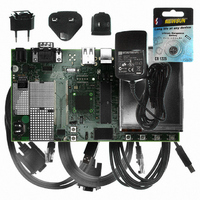
AT91SAM9G10-EK Atmel, AT91SAM9G10-EK Datasheet - Page 350

AT91SAM9G10-EK
Manufacturer Part Number
AT91SAM9G10-EK
Description
KIT DEV FOR SAM9G10 ARM
Manufacturer
Atmel
Type
MCUr
Specifications of AT91SAM9G10-EK
Contents
Board, Cables, Power Supply
Silicon Manufacturer
Atmel
Core Architecture
AVR
Kit Contents
Board
Svhc
No SVHC (15-Dec-2010)
Mcu Supported Families
AT91SAM9G10, ARM926EJ-S
Tool / Board Applications
Microcontroller
Rohs Compliant
Yes
For Use With/related Products
*
Lead Free Status / RoHS Status
Contains lead / RoHS non-compliant
- Current page: 350 of 730
- Download datasheet (12Mb)
Figure 30-4. SPI Transfer Format (NCPHA = 0, 8 bits per transfer)
30.6.3
350
SPCK cycle (for reference)
(from master)
(from slave)
(CPOL = 0)
(CPOL = 1)
(to slave)
AT91SAM9G10
Master Mode Operations
SPCK
SPCK
MOSI
MISO
NSS
*
When configured in Master Mode, the SPI operates on the clock generated by the internal pro-
grammable baud rate generator. It fully controls the data transfers to and from the slave(s)
connected to the SPI bus. The SPI drives the chip select line to the slave and the serial clock
signal (SPCK).
The SPI features two holding registers, the Transmit Data Register and the Receive Data Regis-
ter, and a single Shift Register. The holding registers maintain the data flow at a constant rate.
After enabling the SPI, a data transfer begins when the processor writes to the SPI_TDR (Trans-
mit Data Register). The written data is immediately transferred in the Shift Register and transfer
on the SPI bus starts. While the data in the Shift Register is shifted on the MOSI line, the MISO
line is sampled and shifted in the Shift Register. Receiving data cannot occur without transmit-
ting data. If receiving mode is not needed, for example when communicating with a slave
receiver only (such as an LCD), the receive status flags in the status register can be discarded.
Before writing the TDR, the PCS field in the SPI_MR register must be set in order to select a
slave.
After enabling the SPI, a data transfer begins when the processor writes to the SPI_TDR (Trans-
mit Data Register). The written data is immediately transferred in the Shift Register and transfer
on the SPI bus starts. While the data in the Shift Register is shifted on the MOSI line, the MISO
line is sampled and shifted in the Shift Register. Transmission cannot occur without reception.
Before writing the TDR, the PCS field must be set in order to select a slave.
If new data is written in SPI_TDR during the transfer, it stays in it until the current transfer is
completed. Then, the received data is transferred from the Shift Register to SPI_RDR, the data
in SPI_TDR is loaded in the Shift Register and a new transfer starts.
* Not defined but normally LSB of previous character transmitted.
1
MSB
MSB
2
6
6
3
5
5
4
4
4
5
3
3
6
2
2
7
1
1
8
LSB
6462A–ATARM–03-Jun-09
LSB
Related parts for AT91SAM9G10-EK
Image
Part Number
Description
Manufacturer
Datasheet
Request
R

Part Number:
Description:
MCU, MPU & DSP Development Tools KICKSTART KIT FOR AT91SAM9 PLUS
Manufacturer:
IAR Systems

Part Number:
Description:
DEV KIT FOR AVR/AVR32
Manufacturer:
Atmel
Datasheet:

Part Number:
Description:
INTERVAL AND WIPE/WASH WIPER CONTROL IC WITH DELAY
Manufacturer:
ATMEL Corporation
Datasheet:

Part Number:
Description:
Low-Voltage Voice-Switched IC for Hands-Free Operation
Manufacturer:
ATMEL Corporation
Datasheet:

Part Number:
Description:
MONOLITHIC INTEGRATED FEATUREPHONE CIRCUIT
Manufacturer:
ATMEL Corporation
Datasheet:

Part Number:
Description:
AM-FM Receiver IC U4255BM-M
Manufacturer:
ATMEL Corporation
Datasheet:

Part Number:
Description:
Monolithic Integrated Feature Phone Circuit
Manufacturer:
ATMEL Corporation
Datasheet:

Part Number:
Description:
Multistandard Video-IF and Quasi Parallel Sound Processing
Manufacturer:
ATMEL Corporation
Datasheet:

Part Number:
Description:
High-performance EE PLD
Manufacturer:
ATMEL Corporation
Datasheet:

Part Number:
Description:
8-bit Flash Microcontroller
Manufacturer:
ATMEL Corporation
Datasheet:

Part Number:
Description:
2-Wire Serial EEPROM
Manufacturer:
ATMEL Corporation
Datasheet:


