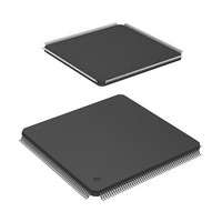
HD6417709SF133B Renesas Electronics America, HD6417709SF133B Datasheet - Page 678

HD6417709SF133B
Manufacturer Part Number
HD6417709SF133B
Description
IC SUPERH MPU ROMLESS 208LQFP
Manufacturer
Renesas Electronics America
Series
SuperH® SH7700r
Datasheet
1.D6417709SBP167BV.pdf
(809 pages)
Specifications of HD6417709SF133B
Core Processor
SH-3
Core Size
32-Bit
Speed
133MHz
Connectivity
EBI/EMI, FIFO, IrDA, SCI, SmartCard
Peripherals
DMA, POR, WDT
Number Of I /o
96
Program Memory Type
ROMless
Ram Size
16K x 8
Voltage - Supply (vcc/vdd)
1.65 V ~ 2.05 V
Data Converters
A/D 8x10b; D/A 2x8b
Oscillator Type
Internal
Operating Temperature
-20°C ~ 75°C
Package / Case
208-LQFP
Lead Free Status / RoHS Status
Contains lead / RoHS non-compliant
Eeprom Size
-
Program Memory Size
-
Available stocks
Company
Part Number
Manufacturer
Quantity
Price
Company:
Part Number:
HD6417709SF133B
Manufacturer:
RENESAS
Quantity:
79
Company:
Part Number:
HD6417709SF133B
Manufacturer:
Renesas Electronics America
Quantity:
10 000
Part Number:
HD6417709SF133B
Manufacturer:
RENESAS/瑞萨
Quantity:
20 000
Part Number:
HD6417709SF133B-V
Manufacturer:
RENESAS/瑞萨
Quantity:
20 000
Part Number:
HD6417709SF133BV
Manufacturer:
RENESAS/瑞萨
Quantity:
20 000
- Current page: 678 of 809
- Download datasheet (5Mb)
20.7
When using the A/D converter, note the following points.
20.7.1
20.7.2
To prevent damage from voltage surges at the analog input pins (AN0 to AN7), connect an input
protection circuit like the one shown in figure 20.9. The circuit shown also includes an CR filter to
suppress noise. This circuit is shown as an example; the circuit constants should be selected
according to actual application conditions. Table 20.5 lists the analog input pin specifications and
figure 20.10 shows an equivalent circuit diagram of the analog input ports.
Rev. 5.00, 09/03, page 632 of 760
Digital output
Analog Input Voltage Range: During A/D conversion, the voltages input to the analog input
pins ANn should be in the range AV
Relationships of AV
V
CC
111
110
101
100
011
010
001
000
± 0.3 V and AV
0 1/8 2/8 3/8 4/8 5/8 6/8 7/8 FS
FS: Full-scale voltage
Usage Notes
Setting Analog Input Voltage
Processing of Analog Input Pins
characteristic
Figure 20.8 Definitions of A/D Conversion Accuracy
conversion
CC
SS
Ideal A/D
(3) Quantization
and AV
= V
error
SS
.
SS
Analog input
: AV
voltage
SS
CC
ANn
and AV
Digital output
AV
SS
characteristic
CC
should be related as follows: AV
conversion
(n = 0 to 7).
(1) Offset error
Ideal A/D
Actual A/D
convertion
characteristic
(4) Nonlinearity
error
(2) Full-scale error
Analog input
voltage
FS
CC
=
Related parts for HD6417709SF133B
Image
Part Number
Description
Manufacturer
Datasheet
Request
R

Part Number:
Description:
KIT STARTER FOR M16C/29
Manufacturer:
Renesas Electronics America
Datasheet:

Part Number:
Description:
KIT STARTER FOR R8C/2D
Manufacturer:
Renesas Electronics America
Datasheet:

Part Number:
Description:
R0K33062P STARTER KIT
Manufacturer:
Renesas Electronics America
Datasheet:

Part Number:
Description:
KIT STARTER FOR R8C/23 E8A
Manufacturer:
Renesas Electronics America
Datasheet:

Part Number:
Description:
KIT STARTER FOR R8C/25
Manufacturer:
Renesas Electronics America
Datasheet:

Part Number:
Description:
KIT STARTER H8S2456 SHARPE DSPLY
Manufacturer:
Renesas Electronics America
Datasheet:

Part Number:
Description:
KIT STARTER FOR R8C38C
Manufacturer:
Renesas Electronics America
Datasheet:

Part Number:
Description:
KIT STARTER FOR R8C35C
Manufacturer:
Renesas Electronics America
Datasheet:

Part Number:
Description:
KIT STARTER FOR R8CL3AC+LCD APPS
Manufacturer:
Renesas Electronics America
Datasheet:

Part Number:
Description:
KIT STARTER FOR RX610
Manufacturer:
Renesas Electronics America
Datasheet:

Part Number:
Description:
KIT STARTER FOR R32C/118
Manufacturer:
Renesas Electronics America
Datasheet:

Part Number:
Description:
KIT DEV RSK-R8C/26-29
Manufacturer:
Renesas Electronics America
Datasheet:

Part Number:
Description:
KIT STARTER FOR SH7124
Manufacturer:
Renesas Electronics America
Datasheet:

Part Number:
Description:
KIT STARTER FOR H8SX/1622
Manufacturer:
Renesas Electronics America
Datasheet:

Part Number:
Description:
KIT DEV FOR SH7203
Manufacturer:
Renesas Electronics America
Datasheet:


