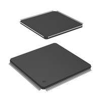
HD6417709SF133B Renesas Electronics America, HD6417709SF133B Datasheet - Page 291

HD6417709SF133B
Manufacturer Part Number
HD6417709SF133B
Description
IC SUPERH MPU ROMLESS 208LQFP
Manufacturer
Renesas Electronics America
Series
SuperH® SH7700r
Datasheet
1.D6417709SBP167BV.pdf
(809 pages)
Specifications of HD6417709SF133B
Core Processor
SH-3
Core Size
32-Bit
Speed
133MHz
Connectivity
EBI/EMI, FIFO, IrDA, SCI, SmartCard
Peripherals
DMA, POR, WDT
Number Of I /o
96
Program Memory Type
ROMless
Ram Size
16K x 8
Voltage - Supply (vcc/vdd)
1.65 V ~ 2.05 V
Data Converters
A/D 8x10b; D/A 2x8b
Oscillator Type
Internal
Operating Temperature
-20°C ~ 75°C
Package / Case
208-LQFP
Lead Free Status / RoHS Status
Contains lead / RoHS non-compliant
Eeprom Size
-
Program Memory Size
-
Available stocks
Company
Part Number
Manufacturer
Quantity
Price
Company:
Part Number:
HD6417709SF133B
Manufacturer:
RENESAS
Quantity:
79
Company:
Part Number:
HD6417709SF133B
Manufacturer:
Renesas Electronics America
Quantity:
10 000
Part Number:
HD6417709SF133B
Manufacturer:
RENESAS/瑞萨
Quantity:
20 000
Part Number:
HD6417709SF133B-V
Manufacturer:
RENESAS/瑞萨
Quantity:
20 000
Part Number:
HD6417709SF133BV
Manufacturer:
RENESAS/瑞萨
Quantity:
20 000
- Current page: 291 of 809
- Download datasheet (5Mb)
10.2.5
The individual memory control register (MCR) is a 16-bit readable/writable register that specifies
RAS and CAS timing for synchronous DRAM (areas 2 and 3), specifies address multiplexing, and
controls refresh. This enables direct connection of synchronous DRAM without external circuits.
MCR is initialized to H'0000 by a power-on reset, but is not initialized by a manual reset or in
standby mode. Bits TPC1–TPC0, RCD1–RCD0, TRWL1–TRWL0, TRAS1–TRAS0, RASD, and
AMX3–AMX0 are written to in the initialization after a power-on reset and should not then be
modified again. When RFSH and RMODE are written to, write the same values to the other bits.
When using synchronous DRAM, do not access areas 2 and 3 until this register is initialized.
Bits 15 and 14—RAS Precharge Time (TPC1, TPC0): When synchronous DRAM interface is
selected as connected memory, they set the minimum number of cycles until output of the next
bank-active command after precharge. However, the number of cycles input immediately after the
issue of an all-bank-precharge command (PALL) in the case of an auto-refresh or a precharge
command (PRE) in the bank active mode is one fewer than the normal value. TPC1 should not be
set to 0 and TPC0 to 1 in the bank active mode.
Note: * Immediately after all-bank-precharge (PALL) in the case of an auto-refresh or precharge
Bit 15:
TPC1
0
1
Initial value:
Initial value:
(PRE) in the bank active mode.
Individual Memory Control Register (MCR)
Bit 14:
TPC0
0
1
0
1
R/W:
R/W:
Bit:
Bit:
RASD
TPC1
R/W
R/W
Normal Operation
1 cycle (Initial value)
2 cycles
3 cycles
4 cycles
15
0
7
0
AMX3
TPC0
R/W
R/W
14
0
6
0
RCD1
AMX2
R/W
R/W
13
0
5
0
Immediately after
Precharge Command *
0 cycle (Initial value)
1 cycle
2 cycles
3 cycles
RCD0
AMX1
R/W
R/W
12
0
4
0
Description
TRWL1 TRWL0
AMX0
R/W
R/W
11
0
3
0
Rev. 5.00, 09/03, page 245 of 760
RFSH
R/W
R/W
10
0
2
0
Immediately after
Self-Refresh
2 cycles (Initial value)
5 cycles
8 cycles
11 cycles
RMODE
TRAS1
R/W
R/W
9
0
1
0
TRAS0
R/W
—
R
8
0
0
0
Related parts for HD6417709SF133B
Image
Part Number
Description
Manufacturer
Datasheet
Request
R

Part Number:
Description:
KIT STARTER FOR M16C/29
Manufacturer:
Renesas Electronics America
Datasheet:

Part Number:
Description:
KIT STARTER FOR R8C/2D
Manufacturer:
Renesas Electronics America
Datasheet:

Part Number:
Description:
R0K33062P STARTER KIT
Manufacturer:
Renesas Electronics America
Datasheet:

Part Number:
Description:
KIT STARTER FOR R8C/23 E8A
Manufacturer:
Renesas Electronics America
Datasheet:

Part Number:
Description:
KIT STARTER FOR R8C/25
Manufacturer:
Renesas Electronics America
Datasheet:

Part Number:
Description:
KIT STARTER H8S2456 SHARPE DSPLY
Manufacturer:
Renesas Electronics America
Datasheet:

Part Number:
Description:
KIT STARTER FOR R8C38C
Manufacturer:
Renesas Electronics America
Datasheet:

Part Number:
Description:
KIT STARTER FOR R8C35C
Manufacturer:
Renesas Electronics America
Datasheet:

Part Number:
Description:
KIT STARTER FOR R8CL3AC+LCD APPS
Manufacturer:
Renesas Electronics America
Datasheet:

Part Number:
Description:
KIT STARTER FOR RX610
Manufacturer:
Renesas Electronics America
Datasheet:

Part Number:
Description:
KIT STARTER FOR R32C/118
Manufacturer:
Renesas Electronics America
Datasheet:

Part Number:
Description:
KIT DEV RSK-R8C/26-29
Manufacturer:
Renesas Electronics America
Datasheet:

Part Number:
Description:
KIT STARTER FOR SH7124
Manufacturer:
Renesas Electronics America
Datasheet:

Part Number:
Description:
KIT STARTER FOR H8SX/1622
Manufacturer:
Renesas Electronics America
Datasheet:

Part Number:
Description:
KIT DEV FOR SH7203
Manufacturer:
Renesas Electronics America
Datasheet:


