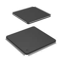
HD6417709SF133B Renesas Electronics America, HD6417709SF133B Datasheet - Page 152

HD6417709SF133B
Manufacturer Part Number
HD6417709SF133B
Description
IC SUPERH MPU ROMLESS 208LQFP
Manufacturer
Renesas Electronics America
Series
SuperH® SH7700r
Datasheet
1.D6417709SBP167BV.pdf
(809 pages)
Specifications of HD6417709SF133B
Core Processor
SH-3
Core Size
32-Bit
Speed
133MHz
Connectivity
EBI/EMI, FIFO, IrDA, SCI, SmartCard
Peripherals
DMA, POR, WDT
Number Of I /o
96
Program Memory Type
ROMless
Ram Size
16K x 8
Voltage - Supply (vcc/vdd)
1.65 V ~ 2.05 V
Data Converters
A/D 8x10b; D/A 2x8b
Oscillator Type
Internal
Operating Temperature
-20°C ~ 75°C
Package / Case
208-LQFP
Lead Free Status / RoHS Status
Contains lead / RoHS non-compliant
Eeprom Size
-
Program Memory Size
-
Available stocks
Company
Part Number
Manufacturer
Quantity
Price
Company:
Part Number:
HD6417709SF133B
Manufacturer:
RENESAS
Quantity:
79
Company:
Part Number:
HD6417709SF133B
Manufacturer:
Renesas Electronics America
Quantity:
10 000
Part Number:
HD6417709SF133B
Manufacturer:
RENESAS/瑞萨
Quantity:
20 000
Part Number:
HD6417709SF133B-V
Manufacturer:
RENESAS/瑞萨
Quantity:
20 000
Part Number:
HD6417709SF133BV
Manufacturer:
RENESAS/瑞萨
Quantity:
20 000
- Current page: 152 of 809
- Download datasheet (5Mb)
5.2.2
CCR2 is used to control the cache-lock function and is valid only in cache locking mode. Cache
locking mode means that the cache lock bit (bit 12) in SR (status register) is set to 1. The cache-
lock function is invalid in non-cache locking mode (the cache-lock bit is 0).
When a prefetch instruction (PREF) is executed in cache locking mode and a cache miss occurs,
one line size of data pointed to by Rn is brought to cache according to the setting of bits 9 and 8
(W3LOAD and W3LOCK) and bits 1 and 0 (W2LOAD and W2LOCK) in CCR2. Table 5.4
shows the relationship between the bit setting and way to be replaced when a prefetch instruction
is executed. When a prefetch instruction is executed and there is a cache hit, new data is not
fetched and an entry which has already been valid is retained. For example, when the cache-lock,
W3LOAD, and W3LOCK bits are set to 1 and a prefetch instruction is executed while one line
size of data pointed to by Rn is already in way 0, a cache hit occurs and data is not fetched to way
3.
When cache is accessed by means of instructions except for a prefetch instruction in cache locking
mode, a way that is replaced by the W3LOCK and W2LOCK bits is restricted. Table 5.5 shows
the relationship between the bit setting of CCR2 and way to be replaced.
The program which modifies the contents of CCR2 must be placed in an address space which does
not cache.
Figure 5.3 shows the configuration of CCR2.
CCR2 is a write-only register; if read, an undefined value will be returned.
Rev. 5.00, 09/03, page 106 of 760
:
CF:
CB:
WT:
CE:
31
Cache Control Register 2 (CCR2)
…
Reserved bits. Always 0 when reading. Data written here is also always 0.
Cache flush bit. Writing 1 flushes all cache entries (clears the V, U, and LRU bits of all
cache entries to 0). Always reads 0. Write-back to external memory is not performed when
the cache is flushed.
Write-back/write-through switchover bit. Indicates the cache’s operating mode for area P1.
1 = write-back mode, 0 = write-through mode.
Write-through bit. Indicates the cache’s operating mode for area P0, U0, and P3.
1 = write-through mode, 0 = write-back mode.
Cache enable bit. Indicates whether the cache function is used.
1 = cache used, 0 = cache not used.
…
…
Figure 5.2 CCR Register Configuration
…
…
…
…
…
6
5
4
CF
3
CB
2
WT
1
CE
0
Related parts for HD6417709SF133B
Image
Part Number
Description
Manufacturer
Datasheet
Request
R

Part Number:
Description:
KIT STARTER FOR M16C/29
Manufacturer:
Renesas Electronics America
Datasheet:

Part Number:
Description:
KIT STARTER FOR R8C/2D
Manufacturer:
Renesas Electronics America
Datasheet:

Part Number:
Description:
R0K33062P STARTER KIT
Manufacturer:
Renesas Electronics America
Datasheet:

Part Number:
Description:
KIT STARTER FOR R8C/23 E8A
Manufacturer:
Renesas Electronics America
Datasheet:

Part Number:
Description:
KIT STARTER FOR R8C/25
Manufacturer:
Renesas Electronics America
Datasheet:

Part Number:
Description:
KIT STARTER H8S2456 SHARPE DSPLY
Manufacturer:
Renesas Electronics America
Datasheet:

Part Number:
Description:
KIT STARTER FOR R8C38C
Manufacturer:
Renesas Electronics America
Datasheet:

Part Number:
Description:
KIT STARTER FOR R8C35C
Manufacturer:
Renesas Electronics America
Datasheet:

Part Number:
Description:
KIT STARTER FOR R8CL3AC+LCD APPS
Manufacturer:
Renesas Electronics America
Datasheet:

Part Number:
Description:
KIT STARTER FOR RX610
Manufacturer:
Renesas Electronics America
Datasheet:

Part Number:
Description:
KIT STARTER FOR R32C/118
Manufacturer:
Renesas Electronics America
Datasheet:

Part Number:
Description:
KIT DEV RSK-R8C/26-29
Manufacturer:
Renesas Electronics America
Datasheet:

Part Number:
Description:
KIT STARTER FOR SH7124
Manufacturer:
Renesas Electronics America
Datasheet:

Part Number:
Description:
KIT STARTER FOR H8SX/1622
Manufacturer:
Renesas Electronics America
Datasheet:

Part Number:
Description:
KIT DEV FOR SH7203
Manufacturer:
Renesas Electronics America
Datasheet:


