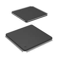
HD6417709SF133B Renesas Electronics America, HD6417709SF133B Datasheet - Page 269

HD6417709SF133B
Manufacturer Part Number
HD6417709SF133B
Description
IC SUPERH MPU ROMLESS 208LQFP
Manufacturer
Renesas Electronics America
Series
SuperH® SH7700r
Datasheet
1.D6417709SBP167BV.pdf
(809 pages)
Specifications of HD6417709SF133B
Core Processor
SH-3
Core Size
32-Bit
Speed
133MHz
Connectivity
EBI/EMI, FIFO, IrDA, SCI, SmartCard
Peripherals
DMA, POR, WDT
Number Of I /o
96
Program Memory Type
ROMless
Ram Size
16K x 8
Voltage - Supply (vcc/vdd)
1.65 V ~ 2.05 V
Data Converters
A/D 8x10b; D/A 2x8b
Oscillator Type
Internal
Operating Temperature
-20°C ~ 75°C
Package / Case
208-LQFP
Lead Free Status / RoHS Status
Contains lead / RoHS non-compliant
Eeprom Size
-
Program Memory Size
-
Available stocks
Company
Part Number
Manufacturer
Quantity
Price
Company:
Part Number:
HD6417709SF133B
Manufacturer:
RENESAS
Quantity:
79
Company:
Part Number:
HD6417709SF133B
Manufacturer:
Renesas Electronics America
Quantity:
10 000
Part Number:
HD6417709SF133B
Manufacturer:
RENESAS/瑞萨
Quantity:
20 000
Part Number:
HD6417709SF133B-V
Manufacturer:
RENESAS/瑞萨
Quantity:
20 000
Part Number:
HD6417709SF133BV
Manufacturer:
RENESAS/瑞萨
Quantity:
20 000
- Current page: 269 of 809
- Download datasheet (5Mb)
10.1
The bus state controller (BSC) divides physical address space and output control signals for
various types of memory and bus interface specifications. BSC functions enable the chip to link
directly with synchronous DRAM, SRAM, ROM, and other memory storage devices without an
external circuit. The BSC also allows direct connection to PCMCIA interfaces, simplifying system
design and allowing high-speed data transfers in a compact system.
10.1.1
The BSC has the following features:
Physical address space is divided into six areas
Direct interface to synchronous DRAM
Burst ROM interface
PCMCIA direct-connection interface
A maximum 64 Mbytes for each of the six areas, 0, 2–6
Area bus width can be selected by register (area 0 is set by external pin)
Wait states can be inserted using the WAIT pin
Wait state insertion can be controlled through software. Register settings can be used to
specify the insertion of 1–10 cycles independently for each area (1–38 cycles for areas 5
and 6 and the PCMCIA interface only)
The type of memory connected can be specified for each area, and control signals are
output for direct memory connection
Wait cycles are automatically inserted to avoid data bus conflict for continuous memory
accesses to different areas or writes directly following reads in the same area
Multiplexes row/column addresses according to synchronous DRAM capacity
Supports burst operation
Supports bank active mode
Has both auto-refresh and self-refresh functions
Controls timing of synchronous DRAM direct-connection control signals according to
register setting
Insertion of wait states controllable through software
Register setting control of burst transfers
Insertion of wait states controllable through software
Bus sizing function for I/O bus width (only in little-endian mode)
Overview
Features
Section 10 Bus State Controller (BSC)
Rev. 5.00, 09/03, page 223 of 760
Related parts for HD6417709SF133B
Image
Part Number
Description
Manufacturer
Datasheet
Request
R

Part Number:
Description:
KIT STARTER FOR M16C/29
Manufacturer:
Renesas Electronics America
Datasheet:

Part Number:
Description:
KIT STARTER FOR R8C/2D
Manufacturer:
Renesas Electronics America
Datasheet:

Part Number:
Description:
R0K33062P STARTER KIT
Manufacturer:
Renesas Electronics America
Datasheet:

Part Number:
Description:
KIT STARTER FOR R8C/23 E8A
Manufacturer:
Renesas Electronics America
Datasheet:

Part Number:
Description:
KIT STARTER FOR R8C/25
Manufacturer:
Renesas Electronics America
Datasheet:

Part Number:
Description:
KIT STARTER H8S2456 SHARPE DSPLY
Manufacturer:
Renesas Electronics America
Datasheet:

Part Number:
Description:
KIT STARTER FOR R8C38C
Manufacturer:
Renesas Electronics America
Datasheet:

Part Number:
Description:
KIT STARTER FOR R8C35C
Manufacturer:
Renesas Electronics America
Datasheet:

Part Number:
Description:
KIT STARTER FOR R8CL3AC+LCD APPS
Manufacturer:
Renesas Electronics America
Datasheet:

Part Number:
Description:
KIT STARTER FOR RX610
Manufacturer:
Renesas Electronics America
Datasheet:

Part Number:
Description:
KIT STARTER FOR R32C/118
Manufacturer:
Renesas Electronics America
Datasheet:

Part Number:
Description:
KIT DEV RSK-R8C/26-29
Manufacturer:
Renesas Electronics America
Datasheet:

Part Number:
Description:
KIT STARTER FOR SH7124
Manufacturer:
Renesas Electronics America
Datasheet:

Part Number:
Description:
KIT STARTER FOR H8SX/1622
Manufacturer:
Renesas Electronics America
Datasheet:

Part Number:
Description:
KIT DEV FOR SH7203
Manufacturer:
Renesas Electronics America
Datasheet:


