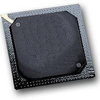
MPC564CZP40 Freescale Semiconductor, MPC564CZP40 Datasheet - Page 986

MPC564CZP40
Manufacturer Part Number
MPC564CZP40
Description
IC MPU 32BIT W/CODE COMP 388PBGA
Manufacturer
Freescale Semiconductor
Series
MPC5xxr
Specifications of MPC564CZP40
Core Processor
PowerPC
Core Size
32-Bit
Speed
40MHz
Connectivity
CAN, EBI/EMI, SCI, SPI, UART/USART
Peripherals
POR, PWM, WDT
Number Of I /o
56
Program Memory Size
512KB (512K x 8)
Program Memory Type
FLASH
Ram Size
32K x 8
Voltage - Supply (vcc/vdd)
2.5 V ~ 2.7 V
Data Converters
A/D 32x10b
Oscillator Type
External
Operating Temperature
-40°C ~ 85°C
Package / Case
388-BGA
Processor Series
MPC5xx
Core
PowerPC
Data Bus Width
32 bit
Data Ram Size
32 KB
Interface Type
CAN, JTAG, QSPI, SCI, SPI, UART
Maximum Clock Frequency
40 MHz
Number Of Programmable I/os
56
Number Of Timers
2
Operating Supply Voltage
0 V to 5 V
Maximum Operating Temperature
+ 85 C
Mounting Style
SMD/SMT
Minimum Operating Temperature
- 40 C
On-chip Adc
2 (10 bit, 32 Channel)
For Use With
MPC564EVB - KIT EVAL FOR MPC561/562/563/564
Lead Free Status / RoHS Status
Contains lead / RoHS non-compliant
Eeprom Size
-
Lead Free Status / Rohs Status
No
Available stocks
Company
Part Number
Manufacturer
Quantity
Price
Company:
Part Number:
MPC564CZP40
Manufacturer:
Freescale Semiconductor
Quantity:
10 000
- Current page: 986 of 1420
- Download datasheet (11Mb)
READI Module
24.6.2
The control and status information is accessed via the four auxiliary access public messages: device ready
for upload/download, upload request (tool requests information), download request (tool provides
information), and upload/download information (device/tool provides information).
To write control or status to memory-mapped locations the following sequence would be required.
24-18
1
1. The tool confirms that the device is ready (so as to not cancel an ongoing read write access). The
2. The tool waits for device ready for upload/download (TCODE 16) message before initiating next
RCPU
23:45
46:47
Bits
Data trace range start and end addresses must be word-aligned.
tool transmits the download request public message (TCODE 18) which contains write attributes,
write data, and target address.
access.
Accessing Memory-Mapped Locations Via
the Auxiliary Port
Nexus
Bits
24:2
1:0
There is no way to distinguish between off-core MPC500 special purpose
register (SPR) map and normal memory map accesses via the defined
address range control. If data trace ranges are set up such that the off-core
MPC500 SPR map falls within active ranges, then accesses to these off-core
MPC500 SPRs will be traced, and the messages will not be distinguishable
from accesses to normal memory map space. Off-core MPC500 SPRs
typically exist in the 8- to 16-Kbyte lowest memory block (0x2000 –
0x3FF0). If data or peripherals are mapped to this space, load/stores to
MPC500 SPRs will be indistinguishable from data or peripheral accesses.
Programmed Values
DTSA
Name
DTSA < DTEA
DTSA > DTEA
DTSA = DTEA
TA
Table 24-15. DTA 1 AND 2 Bit Descriptions (continued)
1
The Read/Write Start Field defines the starting address for the address range.
Refer to
The Read/Write Trace Field can be configured to allow enabling or disabling data read
and/or data write traces.
00 Disable data read and data write trace
x1 Enable data read trace
1x Enable data write trace
MPC561/MPC563 Reference Manual, Rev. 1.2
Table 24-16. Data Trace Values
Table
24-16.
NOTE
DTSA
Range Selected
Word at DTSA
→
Invalid Range
Description
←
DTEA
Freescale Semiconductor
Related parts for MPC564CZP40
Image
Part Number
Description
Manufacturer
Datasheet
Request
R

Part Number:
Description:
MPC5 1K0 5%
Manufacturer:
TE Connectivity
Datasheet:

Part Number:
Description:
MPC5 500R 5%
Manufacturer:
TE Connectivity
Datasheet:

Part Number:
Description:
MPC5 5K0 5%
Manufacturer:
Tyco Electronics
Datasheet:

Part Number:
Description:
MPC5 5R0 5%
Manufacturer:
Tyco Electronics
Datasheet:

Part Number:
Description:
MPC5 50K 5%
Manufacturer:
Tyco Electronics
Datasheet:

Part Number:
Description:
MPC5 1R0 5%
Manufacturer:
Tyco Electronics
Datasheet:
Part Number:
Description:
Manufacturer:
Freescale Semiconductor, Inc
Datasheet:
Part Number:
Description:
Manufacturer:
Freescale Semiconductor, Inc
Datasheet:
Part Number:
Description:
Manufacturer:
Freescale Semiconductor, Inc
Datasheet:
Part Number:
Description:
Manufacturer:
Freescale Semiconductor, Inc
Datasheet:
Part Number:
Description:
Manufacturer:
Freescale Semiconductor, Inc
Datasheet:


