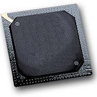
MPC564CZP40 Freescale Semiconductor, MPC564CZP40 Datasheet - Page 669

MPC564CZP40
Manufacturer Part Number
MPC564CZP40
Description
IC MPU 32BIT W/CODE COMP 388PBGA
Manufacturer
Freescale Semiconductor
Series
MPC5xxr
Specifications of MPC564CZP40
Core Processor
PowerPC
Core Size
32-Bit
Speed
40MHz
Connectivity
CAN, EBI/EMI, SCI, SPI, UART/USART
Peripherals
POR, PWM, WDT
Number Of I /o
56
Program Memory Size
512KB (512K x 8)
Program Memory Type
FLASH
Ram Size
32K x 8
Voltage - Supply (vcc/vdd)
2.5 V ~ 2.7 V
Data Converters
A/D 32x10b
Oscillator Type
External
Operating Temperature
-40°C ~ 85°C
Package / Case
388-BGA
Processor Series
MPC5xx
Core
PowerPC
Data Bus Width
32 bit
Data Ram Size
32 KB
Interface Type
CAN, JTAG, QSPI, SCI, SPI, UART
Maximum Clock Frequency
40 MHz
Number Of Programmable I/os
56
Number Of Timers
2
Operating Supply Voltage
0 V to 5 V
Maximum Operating Temperature
+ 85 C
Mounting Style
SMD/SMT
Minimum Operating Temperature
- 40 C
On-chip Adc
2 (10 bit, 32 Channel)
For Use With
MPC564EVB - KIT EVAL FOR MPC561/562/563/564
Lead Free Status / RoHS Status
Contains lead / RoHS non-compliant
Eeprom Size
-
Lead Free Status / Rohs Status
No
Available stocks
Company
Part Number
Manufacturer
Quantity
Price
Company:
Part Number:
MPC564CZP40
Manufacturer:
Freescale Semiconductor
Quantity:
10 000
- Current page: 669 of 1420
- Download datasheet (11Mb)
15.7.6
The RXD1 and RXD2 pins are the receive data pins for the SCI1 and SCI2, respectively. TXD1 and TXD2
are the transmit data pins for the two SCI modules. The pins and their functions are listed in
15.7.7
The SCI can operate in polled or interrupt-driven mode. Status flags in SCxSR reflect SCI conditions
regardless of the operating mode chosen. The TIE, TCIE, RIE, and ILIE bits in SCCxR1 enable interrupts
for the conditions indicated by the TDRE, TC, RDRF, and IDLE bits in SCxSR, respectively.
15.7.7.1
Bit-time
Start bit
Stop bit
Freescale Semiconductor
SRESET
Bits
7:15
0:6
Field
Addr
Transmit Data
Receive Data
SCI Pins
SCI Operation
Pin Names
Definition of Terms
R[8:0]/
Name
T[8:0]
MSB
0
—
1
Reserved
R[7:0]/T[7:0] contain either the eight data bits received when SCxDR is read, or the eight data
bits to be transmitted when SCxDR is written. R8/T8 are used when the SCI is configured for
nine-bit operation (M = 1). When the SCI is configured for 8-bit operation, R8/T8 have no
meaning or effect.
Accesses to the lower byte of SCxDR triggers the mechanism for clearing the status bits or for
initiating transmissions whether byte, half-word, or word accesses are used.
The time required to transmit or receive one bit of data, which is equal to one cycle
of the baud frequency.
One bit-time of logic zero that indicates the beginning of a data frame. A start bit
must begin with a one-to-zero transition and be preceded by at least three receive
time samples of logic one.
One bit-time of logic one that indicates the end of a data frame.
2
0000_000
—
3
RXD1, RXD2
TXD1, TXD2
Figure 15-29. SCI Data Register (SCxDR)
MPC561/MPC563 Reference Manual, Rev. 1.2
Mnemonic
Table 15-27. SCxDR Bit Descriptions
4
Table 15-28. SCI Pin Functions
5
6
R8/T8 R7/T7 R6/T6 R5/T5 R4/T4 R3/T3 R2/T2 R1/T1 R0/T0
Receiver disabled
Receiver enabled
Transmitter disabled
Transmitter enabled
7
0x30 500E
Mode
8
Description
9
10
General purpose input
Serial data input to SCI
General purpose output
Serial data output from SCI
Undefined
11
Queued Serial Multi-Channel Module
Function
12
13
14
Table
LSB
15
15-28.
15-51
Related parts for MPC564CZP40
Image
Part Number
Description
Manufacturer
Datasheet
Request
R

Part Number:
Description:
MPC5 1K0 5%
Manufacturer:
TE Connectivity
Datasheet:

Part Number:
Description:
MPC5 500R 5%
Manufacturer:
TE Connectivity
Datasheet:

Part Number:
Description:
MPC5 5K0 5%
Manufacturer:
Tyco Electronics
Datasheet:

Part Number:
Description:
MPC5 5R0 5%
Manufacturer:
Tyco Electronics
Datasheet:

Part Number:
Description:
MPC5 50K 5%
Manufacturer:
Tyco Electronics
Datasheet:

Part Number:
Description:
MPC5 1R0 5%
Manufacturer:
Tyco Electronics
Datasheet:
Part Number:
Description:
Manufacturer:
Freescale Semiconductor, Inc
Datasheet:
Part Number:
Description:
Manufacturer:
Freescale Semiconductor, Inc
Datasheet:
Part Number:
Description:
Manufacturer:
Freescale Semiconductor, Inc
Datasheet:
Part Number:
Description:
Manufacturer:
Freescale Semiconductor, Inc
Datasheet:
Part Number:
Description:
Manufacturer:
Freescale Semiconductor, Inc
Datasheet:


