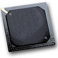
MPC564CZP40 Freescale Semiconductor, MPC564CZP40 Datasheet - Page 918

MPC564CZP40
Manufacturer Part Number
MPC564CZP40
Description
IC MPU 32BIT W/CODE COMP 388PBGA
Manufacturer
Freescale Semiconductor
Series
MPC5xxr
Specifications of MPC564CZP40
Core Processor
PowerPC
Core Size
32-Bit
Speed
40MHz
Connectivity
CAN, EBI/EMI, SCI, SPI, UART/USART
Peripherals
POR, PWM, WDT
Number Of I /o
56
Program Memory Size
512KB (512K x 8)
Program Memory Type
FLASH
Ram Size
32K x 8
Voltage - Supply (vcc/vdd)
2.5 V ~ 2.7 V
Data Converters
A/D 32x10b
Oscillator Type
External
Operating Temperature
-40°C ~ 85°C
Package / Case
388-BGA
Processor Series
MPC5xx
Core
PowerPC
Data Bus Width
32 bit
Data Ram Size
32 KB
Interface Type
CAN, JTAG, QSPI, SCI, SPI, UART
Maximum Clock Frequency
40 MHz
Number Of Programmable I/os
56
Number Of Timers
2
Operating Supply Voltage
0 V to 5 V
Maximum Operating Temperature
+ 85 C
Mounting Style
SMD/SMT
Minimum Operating Temperature
- 40 C
On-chip Adc
2 (10 bit, 32 Channel)
For Use With
MPC564EVB - KIT EVAL FOR MPC561/562/563/564
Lead Free Status / RoHS Status
Contains lead / RoHS non-compliant
Eeprom Size
-
Lead Free Status / Rohs Status
No
Available stocks
Company
Part Number
Manufacturer
Quantity
Price
Company:
Part Number:
MPC564CZP40
Manufacturer:
Freescale Semiconductor
Quantity:
10 000
- Current page: 918 of 1420
- Download datasheet (11Mb)
Development Support
23.1.1.3
There is one special case when although queue flush information is expected on the VF pins, (according
to the last value on the VF pins), regular instruction type information is reported. The only instruction type
information that can appear in this case is VF = 111, branch (direct or indirect) NOT taken. Since the
maximum queue flushes possible is five, it is easy to identify this special case.
23.1.2
When entering debug mode an interrupt/exception taken is reported on the VF pins, (VF = 100) and a cycle
marked with the program trace cycle is made visible externally.
When the CPU is in debug mode, the VF pins equal ‘000’ and the VFLS pins equal ‘11’. For more
information on debug mode refer to
If VSYNC is asserted/negated while the CPU is in debug mode, this information is reported as the first VF
pins report when the CPU returns to regular mode. If VSYNC was not changed while in debug mode. the
first VF pins report will be of an indirect branch taken (VF = 101), suitable for the rfi instruction that is
being issued. In both cases the first instruction fetch after debug mode is marked with the program trace
cycle attribute and therefore is visible externally.
23.1.3
There are cases when non-branch (sequential) instructions may effect the machine in a manner similar to
indirect branch instructions. These instructions include rfi, mtmsr, isync and mtspr to CMPA-F, ICTRL,
ECR and DER.
These instructions are marked by the CPU as indirect branch instructions (VF = 101) and the following
instruction address is marked with the same program trace cycle attribute as if it were an indirect branch
target. Therefore, when one of these special instructions is detected in the CPU, the address of the
following instruction is visible externally. In this way the reconstructing software is able to evaluate
correctly the effect of these instructions.
23.1.4
When program trace is needed, the external hardware needs to sample the status pins (VF and VFLS) each
clock cycle and the address of all cycles marked with the program trace cycle attribute.
23-4
Program Trace when in Debug Mode
Sequential Instructions Marked as Indirect Branch
External Hardware
Queue Flush Information Special Case
VFLS[0:1]
00
01
10
11
MPC561/MPC563 Reference Manual, Rev. 1.2
0 instructions flushed from history queue
1 instruction flushed from history queue
2 instructions flushed from history queue
Used for debug mode indication (FREEZE). Program trace
external hardware should ignore this setting.
Section 23.3, “Development System
Table 23-3. VFLS Pin Encodings
History Buffer Flush Information
Interface.”
Freescale Semiconductor
Related parts for MPC564CZP40
Image
Part Number
Description
Manufacturer
Datasheet
Request
R

Part Number:
Description:
MPC5 1K0 5%
Manufacturer:
TE Connectivity
Datasheet:

Part Number:
Description:
MPC5 500R 5%
Manufacturer:
TE Connectivity
Datasheet:

Part Number:
Description:
MPC5 5K0 5%
Manufacturer:
Tyco Electronics
Datasheet:

Part Number:
Description:
MPC5 5R0 5%
Manufacturer:
Tyco Electronics
Datasheet:

Part Number:
Description:
MPC5 50K 5%
Manufacturer:
Tyco Electronics
Datasheet:

Part Number:
Description:
MPC5 1R0 5%
Manufacturer:
Tyco Electronics
Datasheet:
Part Number:
Description:
Manufacturer:
Freescale Semiconductor, Inc
Datasheet:
Part Number:
Description:
Manufacturer:
Freescale Semiconductor, Inc
Datasheet:
Part Number:
Description:
Manufacturer:
Freescale Semiconductor, Inc
Datasheet:
Part Number:
Description:
Manufacturer:
Freescale Semiconductor, Inc
Datasheet:
Part Number:
Description:
Manufacturer:
Freescale Semiconductor, Inc
Datasheet:


