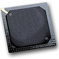
MPC564CZP40 Freescale Semiconductor, MPC564CZP40 Datasheet - Page 814

MPC564CZP40
Manufacturer Part Number
MPC564CZP40
Description
IC MPU 32BIT W/CODE COMP 388PBGA
Manufacturer
Freescale Semiconductor
Series
MPC5xxr
Specifications of MPC564CZP40
Core Processor
PowerPC
Core Size
32-Bit
Speed
40MHz
Connectivity
CAN, EBI/EMI, SCI, SPI, UART/USART
Peripherals
POR, PWM, WDT
Number Of I /o
56
Program Memory Size
512KB (512K x 8)
Program Memory Type
FLASH
Ram Size
32K x 8
Voltage - Supply (vcc/vdd)
2.5 V ~ 2.7 V
Data Converters
A/D 32x10b
Oscillator Type
External
Operating Temperature
-40°C ~ 85°C
Package / Case
388-BGA
Processor Series
MPC5xx
Core
PowerPC
Data Bus Width
32 bit
Data Ram Size
32 KB
Interface Type
CAN, JTAG, QSPI, SCI, SPI, UART
Maximum Clock Frequency
40 MHz
Number Of Programmable I/os
56
Number Of Timers
2
Operating Supply Voltage
0 V to 5 V
Maximum Operating Temperature
+ 85 C
Mounting Style
SMD/SMT
Minimum Operating Temperature
- 40 C
On-chip Adc
2 (10 bit, 32 Channel)
For Use With
MPC564EVB - KIT EVAL FOR MPC561/562/563/564
Lead Free Status / RoHS Status
Contains lead / RoHS non-compliant
Eeprom Size
-
Lead Free Status / Rohs Status
No
Available stocks
Company
Part Number
Manufacturer
Quantity
Price
Company:
Part Number:
MPC564CZP40
Manufacturer:
Freescale Semiconductor
Quantity:
10 000
- Current page: 814 of 1420
- Download datasheet (11Mb)
Peripheral Pin Multiplexing (PPM) Module
The PPM Module has two data transmit signals, PPM_TX[0:1], and two data receive signals,
PPM_RX[0:1]. The amount of data transferred on these signals depends on the setting in
PPMPCR[OP_16_8]. If the PPM is configured to transfer data in 16 PPM_TCLK cycles per 16-bit word
then all data in TX_DATA[0:15] is transmitted on the PPM_TX0 signal, and all data is received into
RX_SHIFTER[0:15] from PPM_RX0. If the PPM is configured to transfer data in eight PPM_TCLK
cycles per 16-bit word then the eight bits will transfer on each of the data transfer signals.
In SPI mode the phase and polarity of PPM_TCLK is selectable by programming bits in the PPMPCR
register. PPM_TCLK can have normal polarity (active high) or inverted polarity (active low). There are
two clock phases available: valid data can be latched on the transition of PPM_TCLK from its active edge
to inactive edge, or valid data can be latched on the transition of PPM_TCLK from its inactive edge to
active edge.
See
settings.
18-8
PPM_TCLK(1)
PPM_TCLK(2)
Section 18.4.2, “PPM Control Register
PPM_TCLK(1) = SYSCLK/4
PPM_TCLK(2) = SYSCLK/2
Update(1)
Update(2)
Update(3)
Update(4)
Update(1) every PPM_TCLK(1)clock
Update(2) every PPM_TCLK(2) clock
Update(3) every second PPM_TCLK(2) clock
Update(4) every fourth PPM_TCLK(2) clock
SYSCLK
SYSCLK
Care must be taken when setting the sample rate with respect to the
OP_16_8 bit setting. For example if the PPM is transferring data on an
8-clock cycle, then setting the sample rate to every 16 clocks will result in
lost data.
Figure 18-7. Examples Of Several TCLK Frequencies and Sample Rates
MPC561/MPC563 Reference Manual, Rev. 1.2
(PPMPCR)” for more information on SPI mode PPM_TCLK
NOTE
Freescale Semiconductor
Related parts for MPC564CZP40
Image
Part Number
Description
Manufacturer
Datasheet
Request
R

Part Number:
Description:
MPC5 1K0 5%
Manufacturer:
TE Connectivity
Datasheet:

Part Number:
Description:
MPC5 500R 5%
Manufacturer:
TE Connectivity
Datasheet:

Part Number:
Description:
MPC5 5K0 5%
Manufacturer:
Tyco Electronics
Datasheet:

Part Number:
Description:
MPC5 5R0 5%
Manufacturer:
Tyco Electronics
Datasheet:

Part Number:
Description:
MPC5 50K 5%
Manufacturer:
Tyco Electronics
Datasheet:

Part Number:
Description:
MPC5 1R0 5%
Manufacturer:
Tyco Electronics
Datasheet:
Part Number:
Description:
Manufacturer:
Freescale Semiconductor, Inc
Datasheet:
Part Number:
Description:
Manufacturer:
Freescale Semiconductor, Inc
Datasheet:
Part Number:
Description:
Manufacturer:
Freescale Semiconductor, Inc
Datasheet:
Part Number:
Description:
Manufacturer:
Freescale Semiconductor, Inc
Datasheet:
Part Number:
Description:
Manufacturer:
Freescale Semiconductor, Inc
Datasheet:


