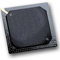
MPC564CZP40 Freescale Semiconductor, MPC564CZP40 Datasheet - Page 227

MPC564CZP40
Manufacturer Part Number
MPC564CZP40
Description
IC MPU 32BIT W/CODE COMP 388PBGA
Manufacturer
Freescale Semiconductor
Series
MPC5xxr
Specifications of MPC564CZP40
Core Processor
PowerPC
Core Size
32-Bit
Speed
40MHz
Connectivity
CAN, EBI/EMI, SCI, SPI, UART/USART
Peripherals
POR, PWM, WDT
Number Of I /o
56
Program Memory Size
512KB (512K x 8)
Program Memory Type
FLASH
Ram Size
32K x 8
Voltage - Supply (vcc/vdd)
2.5 V ~ 2.7 V
Data Converters
A/D 32x10b
Oscillator Type
External
Operating Temperature
-40°C ~ 85°C
Package / Case
388-BGA
Processor Series
MPC5xx
Core
PowerPC
Data Bus Width
32 bit
Data Ram Size
32 KB
Interface Type
CAN, JTAG, QSPI, SCI, SPI, UART
Maximum Clock Frequency
40 MHz
Number Of Programmable I/os
56
Number Of Timers
2
Operating Supply Voltage
0 V to 5 V
Maximum Operating Temperature
+ 85 C
Mounting Style
SMD/SMT
Minimum Operating Temperature
- 40 C
On-chip Adc
2 (10 bit, 32 Channel)
For Use With
MPC564EVB - KIT EVAL FOR MPC561/562/563/564
Lead Free Status / RoHS Status
Contains lead / RoHS non-compliant
Eeprom Size
-
Lead Free Status / Rohs Status
No
Available stocks
Company
Part Number
Manufacturer
Quantity
Price
Company:
Part Number:
MPC564CZP40
Manufacturer:
Freescale Semiconductor
Quantity:
10 000
- Current page: 227 of 1420
- Download datasheet (11Mb)
4.6.2.2
The following registers contain 32 bits and define the starting address of the protected regions. There is
one register for each of four regions.
Freescale Semiconductor
,
HRESET
HRESET
1
2
27:29
20:31
BE and BTEE should not both be set at the same time, setting the BE bit disables the BTB.
This bit is available on the MPC562/MPC564 only, software should write "0" to this bit for MPC561/MPC563.
Bits
Bits
0:19
30
31
Field
Field
Addr
MSB
16
0
Region Base Address Registers (MI_RBA[0:3])
Name
When writing to the BBCMCR register, the following instruction after
mtspr BBCMCR, Rx should be ISYNC, to make sure that the programmed
value will come into effect before any further action.
RA
—
Name
DCAE
Undefined
17
TST
1
—
SPR 784 (MI_RBA0), SPR 785 (MI_RBA1), SPR 786 (MI_RBA2), SPR 787 (MI_RBA3)
RA
Region Base address. The RA field provides the base address of the region. The region base
address should start on the memory block boundary for the corresponding region size, specified
in the region attribute register MI_RA.
Reserved
18
2
Figure 4-8. Region Base Address Register (MI_RBA[0:3])
Table 4-4. BBCMCR Field Descriptions (continued)
Table 4-5. MI_RBA[0:3] Registers Bit Descriptions
Reserved.
NOTE: Bit 27 was BCMEE and should be written as 0.
Decompressor Configuration Access Enable. This bit enables DECRAM and DCCR
registers access from the U-bus master (i.e., RCPU, external master).
0 DECRAM and DCCR registers are locked.
1 DECRAM allows accesses from the U-bus only.
DCAE bit should be set before vocabulary tables are loaded via the U-bus.
Reserved for BBC Test Operations.
19
3
MPC561/MPC563 Reference Manual, Rev. 1.2
20
4
21
5
22
6
NOTE
Unchanged
23
7
RA
Description
24
8
Description
0000_0000_0000
25
9
—
10
26
11
27
Burst Buffer Controller 2 Module
12
28
13
29
14
30
LSB
15
31
4-21
Related parts for MPC564CZP40
Image
Part Number
Description
Manufacturer
Datasheet
Request
R

Part Number:
Description:
MPC5 1K0 5%
Manufacturer:
TE Connectivity
Datasheet:

Part Number:
Description:
MPC5 500R 5%
Manufacturer:
TE Connectivity
Datasheet:

Part Number:
Description:
MPC5 5K0 5%
Manufacturer:
Tyco Electronics
Datasheet:

Part Number:
Description:
MPC5 5R0 5%
Manufacturer:
Tyco Electronics
Datasheet:

Part Number:
Description:
MPC5 50K 5%
Manufacturer:
Tyco Electronics
Datasheet:

Part Number:
Description:
MPC5 1R0 5%
Manufacturer:
Tyco Electronics
Datasheet:
Part Number:
Description:
Manufacturer:
Freescale Semiconductor, Inc
Datasheet:
Part Number:
Description:
Manufacturer:
Freescale Semiconductor, Inc
Datasheet:
Part Number:
Description:
Manufacturer:
Freescale Semiconductor, Inc
Datasheet:
Part Number:
Description:
Manufacturer:
Freescale Semiconductor, Inc
Datasheet:
Part Number:
Description:
Manufacturer:
Freescale Semiconductor, Inc
Datasheet:


