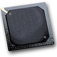
MPC564CZP40 Freescale Semiconductor, MPC564CZP40 Datasheet - Page 421

MPC564CZP40
Manufacturer Part Number
MPC564CZP40
Description
IC MPU 32BIT W/CODE COMP 388PBGA
Manufacturer
Freescale Semiconductor
Series
MPC5xxr
Specifications of MPC564CZP40
Core Processor
PowerPC
Core Size
32-Bit
Speed
40MHz
Connectivity
CAN, EBI/EMI, SCI, SPI, UART/USART
Peripherals
POR, PWM, WDT
Number Of I /o
56
Program Memory Size
512KB (512K x 8)
Program Memory Type
FLASH
Ram Size
32K x 8
Voltage - Supply (vcc/vdd)
2.5 V ~ 2.7 V
Data Converters
A/D 32x10b
Oscillator Type
External
Operating Temperature
-40°C ~ 85°C
Package / Case
388-BGA
Processor Series
MPC5xx
Core
PowerPC
Data Bus Width
32 bit
Data Ram Size
32 KB
Interface Type
CAN, JTAG, QSPI, SCI, SPI, UART
Maximum Clock Frequency
40 MHz
Number Of Programmable I/os
56
Number Of Timers
2
Operating Supply Voltage
0 V to 5 V
Maximum Operating Temperature
+ 85 C
Mounting Style
SMD/SMT
Minimum Operating Temperature
- 40 C
On-chip Adc
2 (10 bit, 32 Channel)
For Use With
MPC564EVB - KIT EVAL FOR MPC561/562/563/564
Lead Free Status / RoHS Status
Contains lead / RoHS non-compliant
Eeprom Size
-
Lead Free Status / Rohs Status
No
Available stocks
Company
Part Number
Manufacturer
Quantity
Price
Company:
Part Number:
MPC564CZP40
Manufacturer:
Freescale Semiconductor
Quantity:
10 000
- Current page: 421 of 1420
- Download datasheet (11Mb)
Note: Timing in this table refers to the typical timing only. Consult the electrical characteristics for exact worst-case timing values.
Additional timing rules not covered in
Freescale Semiconductor
•
•
•
•
•
•
TRLX
1/4 clock actually means 0 to 1/4 clock, 1/2 clock means 1/4 to 1/2 clock.
0
1
1
1
1
1
1
1
1
1
If SETA = 1, an external TA signal is required to terminate the cycle.
If TRLX = 1 and SETA = 1, the minimum cycle length = 3 clock cycles (even if SCY = 0000)
If TRLX = 1, the number of wait states = 2 ∗ SCY & 2 ∗ BSCY
ACS = 01 is not defined (reserved).
If EHTR = 1, an extra (idle) clock cycle is inserted between a read cycle and a following read cycle
to another region, or between a read cycle and a following write cycle to any region.
If LBDIP = 1 (late BDIP assertion), the BDIP signal is asserted only after the number of wait states
for the first beat in a burst have elapsed. See
as well as
Access
Type
write
write
write
write
write
write
write
read
read
read
The LBDIP/TBDIP function can operate only when the cycle termination is
internal, using the number of wait states programmed in one of the ORx
registers. The LBDIP/TBDIP function cannot be activated at the same
time—results are unknown.
Section 9.5.5, “Burst
ACS
11
00
10
11
00
10
11
00
10
11
Table 10-3. Programming Rules for Timing Strobes (continued)
CSNT
X
X
X
1
0
0
0
1
1
1
MPC561/MPC563 Reference Manual, Rev. 1.2
1/2 * clock
(1 + 1/4) *
(1 + 1/2) *
(1 + 1/4) *
(1 + 1/2) *
(1 + 1/4) *
(1 + 1/2) *
Asserted
Address
to CS
clock
clock
clock
clock
clock
clock
0
0
0
Table 10-3
Mechanism.”
Negated to
1/2 * clock
1/4 * clock
1/4 * clock
1/4 * clock
1/4 * clock
1/4 * clock
1/4 * clock
1/4 * clock
Add/Data
(1 + 1/2) *
(1 + 1/2) *
Invalid
clock
clock
CS
NOTE
include the following:
Figure 9-13
Address to
WE/BE or
3/4 * clock
(1 + 3/4) *
(1 + 3/4) *
(1 + 3/4) *
Asserted
3/4 clock
3/4 clock
3/4 clock
(1 + 3/4)
(1 + 3/4)
(1 + 3/4)
clock
clock
clock
clock
clock
clock
OE
in
Chapter 9, “External Bus
Negated to
1/2 * clock
1/4 * clock
1/4 * clock
1/4 * clock
Add/Data
(1 + 1/2) *
(1 + 1/2) *
(1 + 1/2) *
WE/BE
Invalid
clock
clock
clock
X
X
X
Negated to
1/4 * clock
1/4 * clock
1/4 * clock
Add/Data
Invalid
OE
X
X
X
X
X
X
X
Memory Controller
Number of
2 + SCY
2 * SCY
2 * SCY
2 * SCY
2 * SCY
2 * SCY
2 * SCY
2 * SCY
2 * SCY
2 * SCY
Cycles
Interface,”
Total
2 +
3 +
3 +
2 +
3 +
3 +
3 +
4 +
4 +
10-23
Related parts for MPC564CZP40
Image
Part Number
Description
Manufacturer
Datasheet
Request
R

Part Number:
Description:
MPC5 1K0 5%
Manufacturer:
TE Connectivity
Datasheet:

Part Number:
Description:
MPC5 500R 5%
Manufacturer:
TE Connectivity
Datasheet:

Part Number:
Description:
MPC5 5K0 5%
Manufacturer:
Tyco Electronics
Datasheet:

Part Number:
Description:
MPC5 5R0 5%
Manufacturer:
Tyco Electronics
Datasheet:

Part Number:
Description:
MPC5 50K 5%
Manufacturer:
Tyco Electronics
Datasheet:

Part Number:
Description:
MPC5 1R0 5%
Manufacturer:
Tyco Electronics
Datasheet:
Part Number:
Description:
Manufacturer:
Freescale Semiconductor, Inc
Datasheet:
Part Number:
Description:
Manufacturer:
Freescale Semiconductor, Inc
Datasheet:
Part Number:
Description:
Manufacturer:
Freescale Semiconductor, Inc
Datasheet:
Part Number:
Description:
Manufacturer:
Freescale Semiconductor, Inc
Datasheet:
Part Number:
Description:
Manufacturer:
Freescale Semiconductor, Inc
Datasheet:


