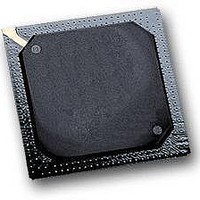
MPC564CZP40 Freescale Semiconductor, MPC564CZP40 Datasheet - Page 156

MPC564CZP40
Manufacturer Part Number
MPC564CZP40
Description
IC MPU 32BIT W/CODE COMP 388PBGA
Manufacturer
Freescale Semiconductor
Series
MPC5xxr
Specifications of MPC564CZP40
Core Processor
PowerPC
Core Size
32-Bit
Speed
40MHz
Connectivity
CAN, EBI/EMI, SCI, SPI, UART/USART
Peripherals
POR, PWM, WDT
Number Of I /o
56
Program Memory Size
512KB (512K x 8)
Program Memory Type
FLASH
Ram Size
32K x 8
Voltage - Supply (vcc/vdd)
2.5 V ~ 2.7 V
Data Converters
A/D 32x10b
Oscillator Type
External
Operating Temperature
-40°C ~ 85°C
Package / Case
388-BGA
Processor Series
MPC5xx
Core
PowerPC
Data Bus Width
32 bit
Data Ram Size
32 KB
Interface Type
CAN, JTAG, QSPI, SCI, SPI, UART
Maximum Clock Frequency
40 MHz
Number Of Programmable I/os
56
Number Of Timers
2
Operating Supply Voltage
0 V to 5 V
Maximum Operating Temperature
+ 85 C
Mounting Style
SMD/SMT
Minimum Operating Temperature
- 40 C
On-chip Adc
2 (10 bit, 32 Channel)
For Use With
MPC564EVB - KIT EVAL FOR MPC561/562/563/564
Lead Free Status / RoHS Status
Contains lead / RoHS non-compliant
Eeprom Size
-
Lead Free Status / Rohs Status
No
Available stocks
Company
Part Number
Manufacturer
Quantity
Price
Company:
Part Number:
MPC564CZP40
Manufacturer:
Freescale Semiconductor
Quantity:
10 000
- Current page: 156 of 1420
- Download datasheet (11Mb)
Central Processing Unit
Unless otherwise noted, reserved fields should be written with a zero when written and return zero when
read. An exception to this rule is XER[16:23]; see
These bits are set to the value written to them and return that value when read.
3.7
The UISA registers can be accessed by either user- or supervisor-level instructions. The general-purpose
registers are accessed through instruction operands.
3.7.1
Integer data is manipulated in the integer unit’s thirty-two 32-bit GPRs, shown below. These registers are
accessed as source and destination registers through operands in the instruction syntax.
3.7.2
The PowerPC ISA architecture provides 32 64-bit FPRs. These registers are accessed as source and
destination registers through operands in floating-point instructions. Each FPR supports the
double-precision, floating-point format. Every instruction that interprets the contents of an FPR as a
3-12
Reset
User Instruction Set Architecture (UISA)
Register Set
General-Purpose Registers (GPRs)
Floating-Point Registers (FPRs)
MSB
0
1 2 3 4 5 6 7 8 9 10 11 12 13 14 15 16 17 18 19 20 21 22 23 24 25 26 27 28 29 30
1
SPR Number
All development-support SPRs are implementation-specific.
(Decimal)
158
159
630
Table 3-3. Development Support SPRs
Figure 3-4. General-Purpose Registers (GPRs)
MPC561/MPC563 Reference Manual, Rev. 1.2
I-bus Support Control Register (ICTRL)
See
Breakpoint Address Register (BAR)
See
Development Port Data Register (DPDR)
See
(DPDR),” for bit descriptions.
Table 23-26
Table 23-28
Section 23.6.13, “Development Port Data Register
Special-Purpose Register
for bit descriptions.
for bit descriptions.
Section 3.7.5, “Integer Exception Register
Unchanged
GPR31
GPR0
GPR1
. . .
. . .
1
(continued)
Freescale Semiconductor
(XER).”
LSB
31
Related parts for MPC564CZP40
Image
Part Number
Description
Manufacturer
Datasheet
Request
R

Part Number:
Description:
MPC5 1K0 5%
Manufacturer:
TE Connectivity
Datasheet:

Part Number:
Description:
MPC5 500R 5%
Manufacturer:
TE Connectivity
Datasheet:

Part Number:
Description:
MPC5 5K0 5%
Manufacturer:
Tyco Electronics
Datasheet:

Part Number:
Description:
MPC5 5R0 5%
Manufacturer:
Tyco Electronics
Datasheet:

Part Number:
Description:
MPC5 50K 5%
Manufacturer:
Tyco Electronics
Datasheet:

Part Number:
Description:
MPC5 1R0 5%
Manufacturer:
Tyco Electronics
Datasheet:
Part Number:
Description:
Manufacturer:
Freescale Semiconductor, Inc
Datasheet:
Part Number:
Description:
Manufacturer:
Freescale Semiconductor, Inc
Datasheet:
Part Number:
Description:
Manufacturer:
Freescale Semiconductor, Inc
Datasheet:
Part Number:
Description:
Manufacturer:
Freescale Semiconductor, Inc
Datasheet:
Part Number:
Description:
Manufacturer:
Freescale Semiconductor, Inc
Datasheet:


