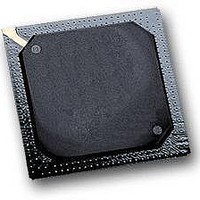
MPC564CZP40 Freescale Semiconductor, MPC564CZP40 Datasheet - Page 702

MPC564CZP40
Manufacturer Part Number
MPC564CZP40
Description
IC MPU 32BIT W/CODE COMP 388PBGA
Manufacturer
Freescale Semiconductor
Series
MPC5xxr
Specifications of MPC564CZP40
Core Processor
PowerPC
Core Size
32-Bit
Speed
40MHz
Connectivity
CAN, EBI/EMI, SCI, SPI, UART/USART
Peripherals
POR, PWM, WDT
Number Of I /o
56
Program Memory Size
512KB (512K x 8)
Program Memory Type
FLASH
Ram Size
32K x 8
Voltage - Supply (vcc/vdd)
2.5 V ~ 2.7 V
Data Converters
A/D 32x10b
Oscillator Type
External
Operating Temperature
-40°C ~ 85°C
Package / Case
388-BGA
Processor Series
MPC5xx
Core
PowerPC
Data Bus Width
32 bit
Data Ram Size
32 KB
Interface Type
CAN, JTAG, QSPI, SCI, SPI, UART
Maximum Clock Frequency
40 MHz
Number Of Programmable I/os
56
Number Of Timers
2
Operating Supply Voltage
0 V to 5 V
Maximum Operating Temperature
+ 85 C
Mounting Style
SMD/SMT
Minimum Operating Temperature
- 40 C
On-chip Adc
2 (10 bit, 32 Channel)
For Use With
MPC564EVB - KIT EVAL FOR MPC561/562/563/564
Lead Free Status / RoHS Status
Contains lead / RoHS non-compliant
Eeprom Size
-
Lead Free Status / Rohs Status
No
Available stocks
Company
Part Number
Manufacturer
Quantity
Price
Company:
Part Number:
MPC564CZP40
Manufacturer:
Freescale Semiconductor
Quantity:
10 000
- Current page: 702 of 1420
- Download datasheet (11Mb)
CAN 2.0B Controller Module
Table 16-7
“Programming
16.3.3
The TouCAN module uses three 8-bit registers to set up the bit timing parameters required by the CAN
protocol. Control registers one and two (CANCTRL1, CANCTRL2) contain the PROPSEG, PSEG1,
PSEG2, and the RJW fields that allow configuration of the bit timing parameters. The prescaler divide
register (PRESDIV) allows selection of the ratio used to derive the serial clock (S-clock) from the system
clock. The time quanta clock operates at the S-clock frequency.
clock, CAN bit rate, and S-clock bit timing parameters, and
16-8
Mask Bit
1
2
3
4
5
6
7
Message Buffer (MB)/Mask
Match for extended format (MB3).
Match for standard format (MB2).
No match for MB3 because of ID0.
No match for MB2 because of ID28.
No match for MB3 because of ID28, match for MB14.
No match for MB14 because of ID27.
Match for MB14.
shows mask examples for normal and extended messages. Refer to
0
1
Bit Timing
Model” for more information on Rx mask registers.
Rx Global Mask
Rx Message In
Rx Message In
Rx 14 Mask
The corresponding incoming ID bit is “don’t care”
The corresponding ID bit is checked against the incoming ID bit to see if a match exists
MB14
MB2
MB3
MB4
MB5
Table 16-7. Mask Examples for Normal/Extended Messages
Table 16-6. Receive Mask Register Bit Values
MPC561/MPC563 Reference Manual, Rev. 1.2
1 1 1 1 1 1 1 1 0 0 0
1 1 1 1 1 1 1 1 0 0 0
0 0 0 0 0 0 1 1 1 1 1
0 0 0 0 0 0 1 1 1 0 1
1 1 1 1 1 1 1 1 0 0 0
1 1 1 1 1 1 1 1 1 1 0
1 1 1 1 1 1 1 1 0 0 1
1 1 1 1 1 1 1 1 0 0 1
1 1 1 1 1 1 1 1 0 0 1
0 1 1 1 1 1 1 1 0 0 0
0 1 1 1 1 1 1 1 0 0 0
0 1 1 1 1 1 1 1 1 1 1
1 0 1 1 1 1 1 1 0 0 0
0 1 1 1 1 1 1 1 0 0 0
ID[28:18]
Base ID
Values
IDE
0
1
0
1
1
1
0
1
0
1
1
1
Figure 16-5
0 1 0 1 0 1 0 1 0 1 0 1 0 1 0 1 0 1
0 1 0 1 0 1 0 1 0 1 0 1 0 1 0 1 0 1
1 1 1 1 1 1 1 0 0 0 0 0 0 0 0 0 0 1
0 1 0 1 0 1 0 1 0 1 0 1 0 1 0 1 0 1
0 1 0 1 0 1 0 1 0 1 0 1 0 1 0 1 0 1
0 1 0 1 0 1 0 1 0 1 0 1 0 1 0 1 0 1
0 1 0 1 0 1 0 1 0 1 0 1 0 1 0 1 0 0
0 1 0 1 0 1 0 1 0 1 0 1 0 1 0 1 0 1
1 1 1 1 1 1 1 0 0 0 0 0 0 0 0 0 0 0
0 1 0 1 0 1 0 1 0 1 0 1 0 1 0 1 0 1
Table 16-8
Extended ID
ID[17:0]
shows the relationship between
—
—
—
—
provides examples of system
Section 16.7,
Freescale Semiconductor
Match
—
14
—
—
—
—
—
—
—
—
—
3
2
—
1
2
3
4
5
6
7
Related parts for MPC564CZP40
Image
Part Number
Description
Manufacturer
Datasheet
Request
R

Part Number:
Description:
MPC5 1K0 5%
Manufacturer:
TE Connectivity
Datasheet:

Part Number:
Description:
MPC5 500R 5%
Manufacturer:
TE Connectivity
Datasheet:

Part Number:
Description:
MPC5 5K0 5%
Manufacturer:
Tyco Electronics
Datasheet:

Part Number:
Description:
MPC5 5R0 5%
Manufacturer:
Tyco Electronics
Datasheet:

Part Number:
Description:
MPC5 50K 5%
Manufacturer:
Tyco Electronics
Datasheet:

Part Number:
Description:
MPC5 1R0 5%
Manufacturer:
Tyco Electronics
Datasheet:
Part Number:
Description:
Manufacturer:
Freescale Semiconductor, Inc
Datasheet:
Part Number:
Description:
Manufacturer:
Freescale Semiconductor, Inc
Datasheet:
Part Number:
Description:
Manufacturer:
Freescale Semiconductor, Inc
Datasheet:
Part Number:
Description:
Manufacturer:
Freescale Semiconductor, Inc
Datasheet:
Part Number:
Description:
Manufacturer:
Freescale Semiconductor, Inc
Datasheet:


