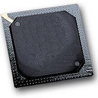
MPC564CZP40 Freescale Semiconductor, MPC564CZP40 Datasheet - Page 530

MPC564CZP40
Manufacturer Part Number
MPC564CZP40
Description
IC MPU 32BIT W/CODE COMP 388PBGA
Manufacturer
Freescale Semiconductor
Series
MPC5xxr
Specifications of MPC564CZP40
Core Processor
PowerPC
Core Size
32-Bit
Speed
40MHz
Connectivity
CAN, EBI/EMI, SCI, SPI, UART/USART
Peripherals
POR, PWM, WDT
Number Of I /o
56
Program Memory Size
512KB (512K x 8)
Program Memory Type
FLASH
Ram Size
32K x 8
Voltage - Supply (vcc/vdd)
2.5 V ~ 2.7 V
Data Converters
A/D 32x10b
Oscillator Type
External
Operating Temperature
-40°C ~ 85°C
Package / Case
388-BGA
Processor Series
MPC5xx
Core
PowerPC
Data Bus Width
32 bit
Data Ram Size
32 KB
Interface Type
CAN, JTAG, QSPI, SCI, SPI, UART
Maximum Clock Frequency
40 MHz
Number Of Programmable I/os
56
Number Of Timers
2
Operating Supply Voltage
0 V to 5 V
Maximum Operating Temperature
+ 85 C
Mounting Style
SMD/SMT
Minimum Operating Temperature
- 40 C
On-chip Adc
2 (10 bit, 32 Channel)
For Use With
MPC564EVB - KIT EVAL FOR MPC561/562/563/564
Lead Free Status / RoHS Status
Contains lead / RoHS non-compliant
Eeprom Size
-
Lead Free Status / Rohs Status
No
Available stocks
Company
Part Number
Manufacturer
Quantity
Price
Company:
Part Number:
MPC564CZP40
Manufacturer:
Freescale Semiconductor
Quantity:
10 000
- Current page: 530 of 1420
- Download datasheet (11Mb)
QADC64E Legacy Mode Operation
13.7
The QADC64E requires accurate, noise-free input signals for proper operation. This section discusses the
design of external circuitry to maximize QADC64E performance.
The QADC64E uses the external signals shown in
be used as general-purpose digital input signals, 8 of which can be configured as either digital input or
output signals.
13.7.1
The 16 port signals on the QADC64E module can be used as analog inputs. Port A signals can be
configured as digital input or digital output signals and Port B signals can be used as 8-bit digital input
signals.
Port A signals are referred to as PQA[7:0] when used as a bidirectional 8-bit digital input/output port.
These eight signals may be used for general-purpose digital input signals or push-pull digital output
signals. Port B signals are referred to as PQB[7:0] when used as digital input signals.
Port A and B signals are connected to a digital input synchronizer during reads and may be used as general
purpose digital inputs when the applied voltages meet high voltage input (V
requirements. Refer to
requirements.
13-66
Trig1
(gate)
EOC
QS
Q1 RES
CF1
TOR1
CWPQ1
CWP
QADC64E Integration Requirements
Port Digital Input/Output Signals
LAST
0
Appendix F, “Electrical
LAST
CCW0
XX
Figure 13-48. Gated Mode, Continuous Scan Timing
8
MPC561/MPC563 Reference Manual, Rev. 1.2
CCW0
CCW1
R0
CCW1
R1
CCW2
Characteristics,” for more information on voltage
Figure
CCW3
CCW2
R2
13-1. There are 16 channel signals that can also
Q restart
CCW3
CCW0
R3
IH
) and low voltage input (V
CCW2
CCW3
R2
Freescale Semiconductor
Q restart
CCW3
CCW0
R3
IL
)
Related parts for MPC564CZP40
Image
Part Number
Description
Manufacturer
Datasheet
Request
R

Part Number:
Description:
MPC5 1K0 5%
Manufacturer:
TE Connectivity
Datasheet:

Part Number:
Description:
MPC5 500R 5%
Manufacturer:
TE Connectivity
Datasheet:

Part Number:
Description:
MPC5 5K0 5%
Manufacturer:
Tyco Electronics
Datasheet:

Part Number:
Description:
MPC5 5R0 5%
Manufacturer:
Tyco Electronics
Datasheet:

Part Number:
Description:
MPC5 50K 5%
Manufacturer:
Tyco Electronics
Datasheet:

Part Number:
Description:
MPC5 1R0 5%
Manufacturer:
Tyco Electronics
Datasheet:
Part Number:
Description:
Manufacturer:
Freescale Semiconductor, Inc
Datasheet:
Part Number:
Description:
Manufacturer:
Freescale Semiconductor, Inc
Datasheet:
Part Number:
Description:
Manufacturer:
Freescale Semiconductor, Inc
Datasheet:
Part Number:
Description:
Manufacturer:
Freescale Semiconductor, Inc
Datasheet:
Part Number:
Description:
Manufacturer:
Freescale Semiconductor, Inc
Datasheet:


