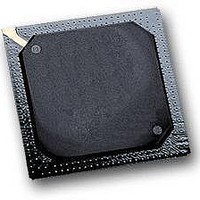
MPC564CZP40 Freescale Semiconductor, MPC564CZP40 Datasheet - Page 114

MPC564CZP40
Manufacturer Part Number
MPC564CZP40
Description
IC MPU 32BIT W/CODE COMP 388PBGA
Manufacturer
Freescale Semiconductor
Series
MPC5xxr
Specifications of MPC564CZP40
Core Processor
PowerPC
Core Size
32-Bit
Speed
40MHz
Connectivity
CAN, EBI/EMI, SCI, SPI, UART/USART
Peripherals
POR, PWM, WDT
Number Of I /o
56
Program Memory Size
512KB (512K x 8)
Program Memory Type
FLASH
Ram Size
32K x 8
Voltage - Supply (vcc/vdd)
2.5 V ~ 2.7 V
Data Converters
A/D 32x10b
Oscillator Type
External
Operating Temperature
-40°C ~ 85°C
Package / Case
388-BGA
Processor Series
MPC5xx
Core
PowerPC
Data Bus Width
32 bit
Data Ram Size
32 KB
Interface Type
CAN, JTAG, QSPI, SCI, SPI, UART
Maximum Clock Frequency
40 MHz
Number Of Programmable I/os
56
Number Of Timers
2
Operating Supply Voltage
0 V to 5 V
Maximum Operating Temperature
+ 85 C
Mounting Style
SMD/SMT
Minimum Operating Temperature
- 40 C
On-chip Adc
2 (10 bit, 32 Channel)
For Use With
MPC564EVB - KIT EVAL FOR MPC561/562/563/564
Lead Free Status / RoHS Status
Contains lead / RoHS non-compliant
Eeprom Size
-
Lead Free Status / Rohs Status
No
Available stocks
Company
Part Number
Manufacturer
Quantity
Price
Company:
Part Number:
MPC564CZP40
Manufacturer:
Freescale Semiconductor
Quantity:
10 000
- Current page: 114 of 1420
- Download datasheet (11Mb)
Signal Descriptions
2-16
MPWM1 / MDO2
MPWM2 / PPM_TX1
MPWM3 / PPM_RX1
MPWM16
MPWM17 / MDO3
MPWM[18:19] / MDO[6:7]
Signal Name
Table 2-1. MPC561/MPC563 Signal Descriptions (continued)
Signals
No. of
1
1
1
1
1
2
MPC561/MPC563 Reference Manual, Rev. 1.2
Type
I/O
I/O
I/O
I/O
I/O
I/O
O
O
O
O
I
MPWM1 unless
the Nexus
(READI) port is
enabled, then
MDO2.
See
MPWM2
MPWM3
MPWM16
MPWM17
unless the
Nexus (READI)
port is enabled.
See
MPWM[18:19]
Function after
Section
Section
Reset
1
2.5.
2.5.
Pulse Width Modulation 1. This signal provides a variable
pulse width output signal at a wide range of frequencies.
READI Message Data Out. Message data out (MDO2) is an
output signal used for uploading OTM, BTM, DTM, and
read/write accesses. External latching of MDO occurs on
the rising edge of MCKO. Eight MDO signals are
implemented.
Pulse Width Modulation 2. This signal provides a variable
pulse width output signal at a wide range of frequencies.
PPMTX1. Transmit data from PPM channel number 1.
Pulse Width Modulation 3. This signal provides a variable
pulse width output signal at a wide range of frequencies.
PPMRX1. Receive data to the PPM channel number 1.
Pulse Width Modulation 16. This signal provides a variable
pulse width output at a wide range of frequencies.
Clock Input: MPWM16 can provide a clock input to modulus
clock submodule, MMCSM8
Pulse Width Modulation 17. This signal provides variable
pulse width outputs at a wide range of frequencies.
Load Input: PWM17 can provide a load input to modulus
clock submodule, MMCSM8
READI Message Data Out. Message data out (MDO3) is an
output signal used for uploading OTM, BTM, DTM, and
read/write accesses. External latching of MDO occurs on
rising edge of MCKO. Eight MDO signals are implemented.
Pulse Width Modulation [18:19]. These signals provide
variable pulse width output signals at a wide range of
frequencies.
Clock and Load Input:
READI Message Data Out. Message data out (MDO[6:7])
are output signals used for uploading OTM, BTM, DTM, and
read/write accesses. External latching of MDO occurs on
rising edge of MCKO. Eight MDO signals are implemented.
• MPWM18 can provide clock inputs to modulus counter
• MPWM19 can provide load inputs to modulus counter
submodule MMCSM24
submodule MMCSM24
Description
Freescale Semiconductor
Related parts for MPC564CZP40
Image
Part Number
Description
Manufacturer
Datasheet
Request
R

Part Number:
Description:
MPC5 1K0 5%
Manufacturer:
TE Connectivity
Datasheet:

Part Number:
Description:
MPC5 500R 5%
Manufacturer:
TE Connectivity
Datasheet:

Part Number:
Description:
MPC5 5K0 5%
Manufacturer:
Tyco Electronics
Datasheet:

Part Number:
Description:
MPC5 5R0 5%
Manufacturer:
Tyco Electronics
Datasheet:

Part Number:
Description:
MPC5 50K 5%
Manufacturer:
Tyco Electronics
Datasheet:

Part Number:
Description:
MPC5 1R0 5%
Manufacturer:
Tyco Electronics
Datasheet:
Part Number:
Description:
Manufacturer:
Freescale Semiconductor, Inc
Datasheet:
Part Number:
Description:
Manufacturer:
Freescale Semiconductor, Inc
Datasheet:
Part Number:
Description:
Manufacturer:
Freescale Semiconductor, Inc
Datasheet:
Part Number:
Description:
Manufacturer:
Freescale Semiconductor, Inc
Datasheet:
Part Number:
Description:
Manufacturer:
Freescale Semiconductor, Inc
Datasheet:


