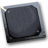
MPC564CZP40 Freescale Semiconductor, MPC564CZP40 Datasheet - Page 737

MPC564CZP40
Manufacturer Part Number
MPC564CZP40
Description
IC MPU 32BIT W/CODE COMP 388PBGA
Manufacturer
Freescale Semiconductor
Series
MPC5xxr
Specifications of MPC564CZP40
Core Processor
PowerPC
Core Size
32-Bit
Speed
40MHz
Connectivity
CAN, EBI/EMI, SCI, SPI, UART/USART
Peripherals
POR, PWM, WDT
Number Of I /o
56
Program Memory Size
512KB (512K x 8)
Program Memory Type
FLASH
Ram Size
32K x 8
Voltage - Supply (vcc/vdd)
2.5 V ~ 2.7 V
Data Converters
A/D 32x10b
Oscillator Type
External
Operating Temperature
-40°C ~ 85°C
Package / Case
388-BGA
Processor Series
MPC5xx
Core
PowerPC
Data Bus Width
32 bit
Data Ram Size
32 KB
Interface Type
CAN, JTAG, QSPI, SCI, SPI, UART
Maximum Clock Frequency
40 MHz
Number Of Programmable I/os
56
Number Of Timers
2
Operating Supply Voltage
0 V to 5 V
Maximum Operating Temperature
+ 85 C
Mounting Style
SMD/SMT
Minimum Operating Temperature
- 40 C
On-chip Adc
2 (10 bit, 32 Channel)
For Use With
MPC564EVB - KIT EVAL FOR MPC561/562/563/564
Lead Free Status / RoHS Status
Contains lead / RoHS non-compliant
Eeprom Size
-
Lead Free Status / Rohs Status
No
Available stocks
Company
Part Number
Manufacturer
Quantity
Price
Company:
Part Number:
MPC564CZP40
Manufacturer:
Freescale Semiconductor
Quantity:
10 000
- Current page: 737 of 1420
- Download datasheet (11Mb)
Every submodule instantiation is also assigned a number. The number of a given submodule is the block
number of the first block of this submodule.
A submodule is assigned a name made of its acronym followed by its submodule number. For example, if
submodule number 18 were an MPWMSM, it would be named MPWMSM18.
This numbering convention does not apply to the MBISM, the MCPSM, and the MIRSMs. The MBISM
and the MCPSM are unique in the MIOS14 and do not need a number. The MIRSMs are numbered
incrementally starting from zero.
The MIOS14 base address is defined at the chip level and is referred to as the “MIOS14 base address.”
The MIOS14 addressable range is four Kbytes.
The base address of a given implemented submodule within the MIOS14 is the sum of the base address of
the MIOS14 and the submodule number multiplied by eight. Refer to
This does not apply to the MBISM, the MCPSM and the MIRSMs. For these submodules, refer to the
MIOS14 memory map in
17.2.2
In
port signals have a prefix of MPIO. The modulus counter clock and load signals are multiplexed with
MDASM signals.
The MIOS14 input and output signal names are composed of five fields according to the following
convention:
The signal prefix and suffix for the different MIOS14 submodules are as follows:
Freescale Semiconductor
Figure
•
•
•
•
•
•
•
“M”
<submodule short_prefix>
<submodule number>
<signal attribute suffix> (optional)
<bit number> (optional)
MMCSM:
— submodule short_prefix: “MC”
— signal attribute suffix: C for the clock signal
— signal attribute suffix: L for the load signal
— For example, an MMCSM placed as submodule number n would have its corresponding input
MDASM:
— submodule short_prefix: “DA”
— signal attribute suffix: none
17-2, MDASM signals have a prefix MDA, MPWMSM signals have a prefix of MPWM and the
clock pin named MMCnC and its input load pin named MMCnL. MMC6C is input on MDA11
and MMC22C is input on MDA13. The MMC6L is input on MDA12 and MMC22C is input
on MDA14.
Signal Naming Convention
Figure
MPC561/MPC563 Reference Manual, Rev. 1.2
17-2.
Table
Modular Input/Output Subsystem (MIOS14)
17-1.
17-5
Related parts for MPC564CZP40
Image
Part Number
Description
Manufacturer
Datasheet
Request
R

Part Number:
Description:
MPC5 1K0 5%
Manufacturer:
TE Connectivity
Datasheet:

Part Number:
Description:
MPC5 500R 5%
Manufacturer:
TE Connectivity
Datasheet:

Part Number:
Description:
MPC5 5K0 5%
Manufacturer:
Tyco Electronics
Datasheet:

Part Number:
Description:
MPC5 5R0 5%
Manufacturer:
Tyco Electronics
Datasheet:

Part Number:
Description:
MPC5 50K 5%
Manufacturer:
Tyco Electronics
Datasheet:

Part Number:
Description:
MPC5 1R0 5%
Manufacturer:
Tyco Electronics
Datasheet:
Part Number:
Description:
Manufacturer:
Freescale Semiconductor, Inc
Datasheet:
Part Number:
Description:
Manufacturer:
Freescale Semiconductor, Inc
Datasheet:
Part Number:
Description:
Manufacturer:
Freescale Semiconductor, Inc
Datasheet:
Part Number:
Description:
Manufacturer:
Freescale Semiconductor, Inc
Datasheet:
Part Number:
Description:
Manufacturer:
Freescale Semiconductor, Inc
Datasheet:


