R0K561622S000BE Renesas Electronics America, R0K561622S000BE Datasheet - Page 768
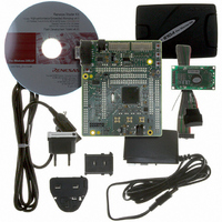
R0K561622S000BE
Manufacturer Part Number
R0K561622S000BE
Description
KIT STARTER FOR H8SX/1622
Manufacturer
Renesas Electronics America
Series
Renesas Starter Kits (RSK)r
Type
MCUr
Specifications of R0K561622S000BE
Contents
Board, Cables, CD, Debugger, Power Supply
Silicon Manufacturer
Renesas
Features
Coding And Debugging, E10A Emulator, RS232 Serial Connection
Kit Contents
Board
Silicon Family Name
H8SX/1622F
Silicon Core Number
R5F61622N50LGV
Lead Free Status / RoHS Status
Lead free / RoHS Compliant
For Use With/related Products
H8SX/1622
Lead Free Status / RoHS Status
Lead free / RoHS Compliant, Lead free / RoHS Compliant


Section 18 A/D Converter
18.7.7
If the conditions shown below are not met, the reliability of the LSI may be adversely affected.
• Analog input voltage range
• Relation between AVcc, AVss and Vcc, Vss
• Vref setting range
18.7.8
In board design, digital circuitry and analog circuitry should be as mutually isolated as possible,
and layout in which digital circuit signal lines and analog circuit signal lines cross or are in close
proximity should be avoided as far as possible. Failure to do so may result in incorrect operation
of the analog circuitry due to inductance, adversely affecting A/D conversion values.
Digital circuitry must be isolated from the analog input pins (AN0 to AN7), analog reference
power supply (Vref), and analog power supply (AVcc) by the analog ground (AVss). Also, the
analog ground (AVss) should be connected at one point to a stable ground (Vss) on the board.
18.7.9
A protection circuit connected to prevent damage due to an abnormal voltage such as an excessive
surge at the analog input pins (AN0 to AN7) should be connected between AVcc and AVss as
shown in figure 18.13. Also, the bypass capacitors connected to AVcc and the filter capacitor
connected to the AN0 to AN7 pins must be connected to AVss.
If a filter capacitor is connected, the input currents at the AN0 to AN7 pins are averaged, and so an
error may arise. Also, when A/D conversion is performed frequently, as in scan mode, if the
current charged and discharged by the capacitance of the sample-and-hold circuit in the A/D
converter exceeds the current input via the input impedance (R
input pin voltage. Careful consideration is therefore required when deciding the circuit constants.
Rev. 2.00 Sep. 16, 2009 Page 738 of 1036
REJ09B0414-0200
The voltage applied to analog input pin ANn during A/D conversion should be in the range
AVss ≤ V
As the relationship between AVcc, AVss and Vcc, Vss, set AVcc = Vcc ± 0.3 V and AVss =
Vss. If the A/D converter is not used, set AVcc = Vcc and AVss = Vss.
The reference voltage at the Vref pin should be set in the range Vref ≤ AVcc.
Setting Range of Analog Power Supply and Other Pins
Notes on Board Design
Notes on Countermeasure against Noise
AN
≤ Vref.
in
), an error will arise in the analog
Related parts for R0K561622S000BE
Image
Part Number
Description
Manufacturer
Datasheet
Request
R

Part Number:
Description:
KIT STARTER FOR M16C/29
Manufacturer:
Renesas Electronics America
Datasheet:

Part Number:
Description:
KIT STARTER FOR R8C/2D
Manufacturer:
Renesas Electronics America
Datasheet:

Part Number:
Description:
R0K33062P STARTER KIT
Manufacturer:
Renesas Electronics America
Datasheet:

Part Number:
Description:
KIT STARTER FOR R8C/23 E8A
Manufacturer:
Renesas Electronics America
Datasheet:

Part Number:
Description:
KIT STARTER FOR R8C/25
Manufacturer:
Renesas Electronics America
Datasheet:

Part Number:
Description:
KIT STARTER H8S2456 SHARPE DSPLY
Manufacturer:
Renesas Electronics America
Datasheet:

Part Number:
Description:
KIT STARTER FOR R8C38C
Manufacturer:
Renesas Electronics America
Datasheet:

Part Number:
Description:
KIT STARTER FOR R8C35C
Manufacturer:
Renesas Electronics America
Datasheet:

Part Number:
Description:
KIT STARTER FOR R8CL3AC+LCD APPS
Manufacturer:
Renesas Electronics America
Datasheet:
Part Number:
Description:
KIT STARTER FOR RX610
Manufacturer:
Renesas Electronics America
Datasheet:

Part Number:
Description:
KIT STARTER FOR R32C/118
Manufacturer:
Renesas Electronics America
Datasheet:

Part Number:
Description:
KIT DEV RSK-R8C/26-29
Manufacturer:
Renesas Electronics America
Datasheet:

Part Number:
Description:
KIT STARTER FOR SH7124
Manufacturer:
Renesas Electronics America
Datasheet:

Part Number:
Description:
KIT DEV FOR SH7203
Manufacturer:
Renesas Electronics America
Datasheet:
Part Number:
Description:
KIT STARTER FOR R8C/18191A1B
Manufacturer:
Renesas Electronics America
Datasheet: