R0K561622S000BE Renesas Electronics America, R0K561622S000BE Datasheet - Page 730
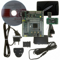
R0K561622S000BE
Manufacturer Part Number
R0K561622S000BE
Description
KIT STARTER FOR H8SX/1622
Manufacturer
Renesas Electronics America
Series
Renesas Starter Kits (RSK)r
Type
MCUr
Specifications of R0K561622S000BE
Contents
Board, Cables, CD, Debugger, Power Supply
Silicon Manufacturer
Renesas
Features
Coding And Debugging, E10A Emulator, RS232 Serial Connection
Kit Contents
Board
Silicon Family Name
H8SX/1622F
Silicon Core Number
R5F61622N50LGV
Lead Free Status / RoHS Status
Lead free / RoHS Compliant
For Use With/related Products
H8SX/1622
Lead Free Status / RoHS Status
Lead free / RoHS Compliant, Lead free / RoHS Compliant


Section 17 I
17.4.3
In master receive mode, the master device outputs the receive clock, receives data from the slave
device, and returns an acknowledge signal. Figures 17.7 and 17.8 show the operation timings in
master receive mode. The reception procedure and operations in master receive mode are shown
below.
1. Clear the TEND bit in ICSR to 0, then clear the TRS bit in ICCRA to 0 to switch from master
2. When ICDDR is read (dummy read), reception is started, the receive clock pulse is output, and
3. After the reception of the first frame data is completed, the RDRF bit in ICSR is set to 1 at the
4. The continuous reception is performed by reading ICDRR and clearing RDRF to 0 every time
5. If the next frame is the last receive data, set the RCVD bit in ICCR1 before reading ICDRR.
6. When the RDRF bit is set to 1 at the rising of the ninth receive clock pulse, the stop condition
7. When the STOP bit in ICSR is set to 1, read ICDRR and clear RCVD to 0.
8. The operation returns to the slave receive mode.
Rev. 2.00 Sep. 16, 2009 Page 700 of 1036
REJ09B0414-0200
transmit mode to master receive mode. Then, clear the TDRE bit to 0.
data is received, in synchronization with the internal clock. The master mode outputs the level
specified by the ACKBT in ICIER to SDA, at the ninth receive clock pulse.
rising of the ninth receive clock pulse. At this time, the received data is read by reading
ICDRR. At the same time, RDRF is cleared.
RDRF is set. If the eighth receive clock pulse falls after reading ICDRR by other processing
while RDRF is 1, SCL is fixed to a low level until ICDRR is read.
This enables the issuance of the stop condition after the next reception.
is issued.
Master Receive Operation
2
C Bus Interface 2 (IIC2)
Related parts for R0K561622S000BE
Image
Part Number
Description
Manufacturer
Datasheet
Request
R

Part Number:
Description:
KIT STARTER FOR M16C/29
Manufacturer:
Renesas Electronics America
Datasheet:

Part Number:
Description:
KIT STARTER FOR R8C/2D
Manufacturer:
Renesas Electronics America
Datasheet:

Part Number:
Description:
R0K33062P STARTER KIT
Manufacturer:
Renesas Electronics America
Datasheet:

Part Number:
Description:
KIT STARTER FOR R8C/23 E8A
Manufacturer:
Renesas Electronics America
Datasheet:

Part Number:
Description:
KIT STARTER FOR R8C/25
Manufacturer:
Renesas Electronics America
Datasheet:

Part Number:
Description:
KIT STARTER H8S2456 SHARPE DSPLY
Manufacturer:
Renesas Electronics America
Datasheet:

Part Number:
Description:
KIT STARTER FOR R8C38C
Manufacturer:
Renesas Electronics America
Datasheet:

Part Number:
Description:
KIT STARTER FOR R8C35C
Manufacturer:
Renesas Electronics America
Datasheet:

Part Number:
Description:
KIT STARTER FOR R8CL3AC+LCD APPS
Manufacturer:
Renesas Electronics America
Datasheet:
Part Number:
Description:
KIT STARTER FOR RX610
Manufacturer:
Renesas Electronics America
Datasheet:

Part Number:
Description:
KIT STARTER FOR R32C/118
Manufacturer:
Renesas Electronics America
Datasheet:

Part Number:
Description:
KIT DEV RSK-R8C/26-29
Manufacturer:
Renesas Electronics America
Datasheet:

Part Number:
Description:
KIT STARTER FOR SH7124
Manufacturer:
Renesas Electronics America
Datasheet:

Part Number:
Description:
KIT DEV FOR SH7203
Manufacturer:
Renesas Electronics America
Datasheet:
Part Number:
Description:
KIT STARTER FOR R8C/18191A1B
Manufacturer:
Renesas Electronics America
Datasheet: