R0K561622S000BE Renesas Electronics America, R0K561622S000BE Datasheet - Page 639
R0K561622S000BE
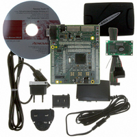
Manufacturer Part Number
R0K561622S000BE
Description
KIT STARTER FOR H8SX/1622
Manufacturer
Renesas Electronics America
Series
Renesas Starter Kits (RSK)r
Type
MCUr
Specifications of R0K561622S000BE
Contents
Board, Cables, CD, Debugger, Power Supply
Silicon Manufacturer
Renesas
Features
Coding And Debugging, E10A Emulator, RS232 Serial Connection
Kit Contents
Board
Silicon Family Name
H8SX/1622F
Silicon Core Number
R5F61622N50LGV
Lead Free Status / RoHS Status
Lead free / RoHS Compliant
For Use With/related Products
H8SX/1622
Lead Free Status / RoHS Status
Lead free / RoHS Compliant, Lead free / RoHS Compliant


Bit Functions in Smart Card Interface Mode (When SMIF in SCMR = 1):
Bit
7
6
5
4
3
2
Bit Name
GM
BLK
PE
O/E
BCP1
BCP0
Initial
Value
0
0
0
0
0
0
R/W
R/W
R/W
R/W
R/W
R/W
R/W
Description
GSM Mode
Setting this bit to 1 allows GSM mode operation. In
GSM mode, the TEND set timing is put forward to 11.0
etu from the start and the clock output control function
is appended. For details, see sections 16.7.6, Data
Transmission (Except in Block Transfer Mode) and
16.7.8, Clock Output Control.
Setting this bit to 1 allows block transfer mode
operation. For details, see section 16.7.3, Block
Transfer Mode.
Parity Enable (valid only in asynchronous mode)
When this bit is set to 1, the parity bit is added to
transmit data before transmission, and the parity bit is
checked in reception. Set this bit to 1 in smart card
interface mode.
Parity Mode (valid only when the PE bit is 1 in
asynchronous mode)
0: Selects even parity
1: Selects odd parity
For details on the usage of this bit in smart card
interface mode, see section 16.7.2, Data Format
(Except in Block Transfer Mode).
Basic Clock Pulse 1,0
These bits select the number of basic clock cycles in a
1-bit data transfer time in smart card interface mode.
00: 32 clock cycles (S = 32)
01: 64 clock cycles (S = 64)
10: 372 clock cycles (S = 372)
11: 256 clock cycles (S = 256)
For details, see section 16.7.4, Receive Data Sampling
Timing and Reception Margin. S is described in section
16.3.9, Bit Rate Register (BRR).
Section 16 Serial Communication Interface (SCI)
Rev. 2.00 Sep. 16, 2009 Page 609 of 1036
REJ09B0414-0200
Related parts for R0K561622S000BE
Image
Part Number
Description
Manufacturer
Datasheet
Request
R

Part Number:
Description:
KIT STARTER FOR M16C/29
Manufacturer:
Renesas Electronics America
Datasheet:

Part Number:
Description:
KIT STARTER FOR R8C/2D
Manufacturer:
Renesas Electronics America
Datasheet:

Part Number:
Description:
R0K33062P STARTER KIT
Manufacturer:
Renesas Electronics America
Datasheet:

Part Number:
Description:
KIT STARTER FOR R8C/23 E8A
Manufacturer:
Renesas Electronics America
Datasheet:

Part Number:
Description:
KIT STARTER FOR R8C/25
Manufacturer:
Renesas Electronics America
Datasheet:

Part Number:
Description:
KIT STARTER H8S2456 SHARPE DSPLY
Manufacturer:
Renesas Electronics America
Datasheet:

Part Number:
Description:
KIT STARTER FOR R8C38C
Manufacturer:
Renesas Electronics America
Datasheet:

Part Number:
Description:
KIT STARTER FOR R8C35C
Manufacturer:
Renesas Electronics America
Datasheet:

Part Number:
Description:
KIT STARTER FOR R8CL3AC+LCD APPS
Manufacturer:
Renesas Electronics America
Datasheet:
Part Number:
Description:
KIT STARTER FOR RX610
Manufacturer:
Renesas Electronics America
Datasheet:

Part Number:
Description:
KIT STARTER FOR R32C/118
Manufacturer:
Renesas Electronics America
Datasheet:

Part Number:
Description:
KIT DEV RSK-R8C/26-29
Manufacturer:
Renesas Electronics America
Datasheet:

Part Number:
Description:
KIT STARTER FOR SH7124
Manufacturer:
Renesas Electronics America
Datasheet:

Part Number:
Description:
KIT DEV FOR SH7203
Manufacturer:
Renesas Electronics America
Datasheet:
Part Number:
Description:
KIT STARTER FOR R8C/18191A1B
Manufacturer:
Renesas Electronics America
Datasheet: